Engineers across industries are actively exploring how Gallium Nitride (GaN) is reshaping power electronics design. To better understand what is really happening in GaN adoption today – and the challenges designers face along the way – EPC – Efficient Power Conversion has launched a short industry survey.
The goal is simple: gather real feedback from engineers who are already working with GaN or evaluating the transition from silicon. Their insights will help identify current obstacles, opportunities, and priorities in next-generation power conversion design.
The survey takes just 2–3 minutes to complete and participants will receive access to key insights from the upcoming GaN adoption report.
By contributing your perspective, you help strengthen a shared understanding of where the technology stands today – and where it is going next.
For more than four decades, the silicon power MOSFET has been the dominant device for low- and medium-voltage power conversion. Its widespread adoption has been driven by a mature manufacturing ecosystem, predictable electrical behavior, and relative ease of integration into electronic systems. From consumer electronics and telecommunications infrastructure to industrial power supplies and automotive electronics, MOSFETs have long represented the most practical solution for efficient power switching. Over time, architectural improvements such as trench structures and superjunction technologies have enabled steady performance gains, particularly in reducing conduction losses while maintaining voltage capability.
However, silicon MOSFET technology is now approaching its fundamental physical limits. As modern electronics demand higher efficiency, increased power density, and faster switching performance, traditional silicon devices face growing challenges. These constraints have opened the door for wide-bandgap semiconductor technologies, particularly gallium nitride (GaN), which are redefining what is possible in power electronics.
One of the long-standing challenges with silicon MOSFETs lies in the trade-off between conduction losses and switching losses. Achieving lower conduction resistance often requires larger device structures, which in turn increase parasitic capacitances. These capacitances slow switching transitions and increase switching losses, especially at higher frequencies. As a result, designers have historically had to operate converters at relatively modest switching frequencies to maintain acceptable efficiency. This compromise has shaped the design of power electronics systems for decades.
Gallium nitride devices address many of these limitations by leveraging fundamentally different material properties. GaN belongs to a class of materials known as wide-bandgap semiconductors, which possess characteristics that enable superior electrical performance compared with conventional silicon. In particular, GaN can sustain much stronger electric fields before breakdown occurs. This capability allows power devices to be built with significantly thinner structures while still supporting high voltages.
Because of these material advantages, GaN transistors can achieve extremely low resistance while maintaining compact device geometries. Smaller structures naturally lead to lower capacitances, enabling faster switching transitions and significantly reducing switching losses. The combination of low resistance and fast switching allows GaN devices to operate efficiently at much higher frequencies than traditional silicon MOSFETs.
Another key advantage of GaN technology is the absence of reverse-recovery charge. In silicon MOSFETs, the body diode can generate significant reverse-recovery losses during switching events, particularly in hard-switching converter topologies. GaN devices largely eliminate this effect, which further improves efficiency and reduces energy loss during switching transitions.
The ability to operate efficiently at higher switching frequencies has profound implications at the system level. In traditional power converters, large passive components such as inductors and transformers often dominate the size and weight of the system. These components are directly related to switching frequency: higher frequencies allow smaller magnetics and reduced filtering requirements.
By enabling switching frequencies well into the megahertz range, GaN technology allows designers to dramatically shrink the size of power supplies. The result is higher power density, lighter systems, and faster dynamic response. These advantages are especially valuable in emerging applications such as AI data centers, robotics, advanced automotive electronics, and high-performance computing platforms, where both efficiency and compact design are critical.
GaN technology is also enabling new levels of integration in power electronics. Many GaN devices are built using lateral structures that support advanced packaging techniques, including chip-scale packages and highly integrated power stages. In some designs, drivers, sensing elements, and control circuitry can be combined with the power devices themselves, simplifying system design and reducing the overall component count.
Although GaN devices may still carry a higher component-level cost than silicon MOSFETs in some applications, system-level benefits often outweigh this difference. Reduced passive component size, improved efficiency, and simplified circuit architectures can lower the total system cost while simultaneously improving performance.
As electronic systems continue to demand greater efficiency and higher power density, the shift toward wide-bandgap technologies is accelerating. Silicon MOSFETs will continue to play an important role in many established applications thanks to their mature ecosystem and cost advantages. However, GaN is rapidly gaining ground in the most demanding and fastest-growing segments of the power electronics market.
From fast chargers and 48-V power architectures to AI data centers and high-frequency DC-DC converters, GaN is enabling a new generation of compact, efficient, and high-performance power systems.
All major optical building blocks of QKD integrated on photonic chips, enabling scalable, cost-efficient quantum-secure communications for real-world networks
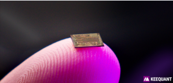
KEEQuant today announced the launch of its commercial-grade chip-scale QKD technology, marking a major advance in quantum-secure communications. This innovation significantly reshapes both the cost structure and the practical deployment of quantum key distribution by replacing large and complex optical subsystems with integrated photonic technologies. As a result, quantum-secure key exchange is becoming a feasible upgrade path for telecom operators, data center operators, and organizations managing critical infrastructure. The approach enables more compact, scalable, and cost-effective implementations while maintaining interoperability with existing fiber networks and established encryption frameworks. This improved compatibility makes large-scale adoption considerably more achievable for organizations seeking to strengthen their infrastructure against the long-term security challenges expected from the evolution of quantum computing.
“For years, QKD has been seen as strategically important, but too complex and too costly for broad deployment,” said Imran Khan, Managing Director at KEEQuant. “Bringing QKD to the chip scale changes that. It gives quantum-safe key exchange the economics and practicality it needs to move into real-world networks.”
Based on this technology, KEEQuant will begin shipments to first customers later this year.
Why chip-scale QKD is a market inflection point:
A dramatically lower system-cost basis fundamentally changes the economics of QKD
Wider accessibility makes quantum-safe key exchange viable for many more applications and customers
Broader market adoption becomes possible as QKD moves beyond premium niche deployments
New business models and integration opportunities open up across communications, security and quantum-network infrastructure
Technically, the milestone is the integration and system-level validation of the major optical building blocks required for QKD on photonic chips. Using commercial PICs, KEEQuant brought transmitter and receiver lasers, modulation, receiver optics and detection to the chip scale, replacing bulky optical assemblies with a compact photonic architecture. Beyond miniaturization alone, this establishes the engineering basis for repeatable packaging, manufacturable system design and reliable system-level integration of chip-scale QKD building blocks.
With this launch, KEEQuant moves quantum-safe communications from research and pilot deployments into commercially viable infrastructure.
Traction inverters are a crucial component of electric vehicles (EVs), responsible for converting direct current (DC) power from the battery into alternating current (AC) power to drive the electric motors. They play a vital role in controlling the speed and torque of the EV’s motors, making them essential for efficient and smooth operation.
Main vs. auxiliary inverters
In most EVs, there are two types of inverters: the main inverter and the auxiliary inverter.
Main inverter: The main inverter is the primary inverter in the EV, responsible for driving the main traction motor. It handles the majority of the power required to propel the vehicle.
Auxiliary inverter: The auxiliary inverter is a smaller inverter that is used to power the vehicle’s auxiliary systems, such as the air conditioning, power steering, and infotainment systems.
The main inverter is typically a much larger and more powerful inverter than the auxiliary inverter. It is designed to handle the high currents and voltages required to drive the main traction motor. The auxiliary inverter, on the other hand, is designed to handle lower currents and voltages, as it is only responsible for powering the vehicle’s auxiliary systems.
Key components of a traction inverter
A traction inverter is a critical component in electric vehicles (EVs), responsible for converting the direct current (DC) from the vehicle’s battery pack into the alternating current (AC) required by the electric motor. Understanding its key components is essential for grasping how EVs operate efficiently.
Power semiconductor devices
At the heart of the traction inverter are the power semiconductor devices, which include insulated-gate bipolar transistors (IGBTs) or silicon carbide (SiC) metal-oxide-semiconductor field-effect transistors (MOSFETs). These devices play a vital role in high-frequency switching, enabling the conversion of DC input into the desired AC waveform. Their performance directly influences the efficiency and responsiveness of the entire inverter system.
Gate drive circuitry
Complementing the power semiconductor devices is the gate drive circuitry. This component is responsible for providing the appropriate control signals that ensure the semiconductor devices switch on and off at the right times. Proper timing is crucial, as it determines the inverter’s ability to generate a smooth and effective AC output for the motor.
DC-link capacitor
The DC-link capacitor serves as a filter for the DC input from the battery pack. By smoothing out any ripple or fluctuations in voltage, it helps maintain a stable and consistent input to the power semiconductor devices. This stability is essential for reliable inverter operation and contributes to the overall performance of the vehicle.
Cooling system
Given that the traction inverter generates a significant amount of heat during operation, an effective cooling system is essential. This typically includes a heatsink, fan, and/or liquid cooling system designed to dissipate heat and keep the inverter’s operating temperature within an acceptable range. Efficient cooling ensures the longevity and reliability of the inverter.
Control and monitoring circuitry
The control and monitoring circuitry manages the overall operation of the traction inverter. This includes controlling the switching of the power semiconductor devices, monitoring temperature and current levels, and providing feedback to the vehicle’s main control system. This component is crucial for maintaining optimal performance and safety.
EMI/EMC filtering
The high-frequency switching in traction inverters can generate electromagnetic interference (EMI), potentially disrupting other vehicle systems. Effective EMI/EMC (electromagnetic compatibility) filtering is necessary to ensure that the inverter operates without causing interference, contributing to the smooth functioning of the entire vehicle.
Packaging and integration
Finally, the design and packaging of the traction inverter play a crucial role in optimizing its performance, efficiency, and reliability. Proper integration with the vehicle’s powertrain and electrical systems ensures that the inverter operates seamlessly within the overall architecture of the EV.
Figure 1 shows the block diagram of a typical main traction inverter for electric vehicles.
Figure 1: Block diagram of a typical main traction inverter (Source: STMicroelectronics)
Traction inverter topologies
Traction inverters play a crucial role in electric vehicles (EVs) by converting direct current (DC) from the battery into alternating current (AC) to drive the electric motor. There are several different topologies for traction inverters, each with its advantages and disadvantages. The most common topologies are listed hereafter.
Two-level topology
The two-level topology is the most prevalent design for traction inverters. It is characterized by its simplicity and cost-effectiveness, making it a popular choice for many applications. This topology typically consists of a basic inverter circuit that switches between two voltage levels, which allows for straightforward control of the motor. However, while it is easy to implement, it may not provide the highest efficiency or the lowest harmonic distortion compared to more complex designs.
Three-level topology
The three-level topology enhances the performance of traction inverters by introducing an additional voltage level. This design can significantly improve the efficiency of the inverter and reduce the harmonic distortion of the AC waveform produced. By utilizing three voltage levels, the inverter can create a smoother output waveform, which is beneficial for the operation of electric motors. This topology also allows for better thermal management and can reduce the stress on the switching devices, leading to improved reliability.
Multilevel topology
Multilevel inverters (MLIs) represent an advanced approach to traction inverter design. These systems can further enhance efficiency and minimize harmonic distortion by using multiple voltage levels—often more than three. The increased number of levels allows for a more refined output waveform, which can lead to better performance in terms of torque and speed control of the electric motor. Additionally, multilevel topologies can distribute power losses more evenly across the switching devices, which can improve the overall thermal performance and lifespan of the inverter.
The choice of traction inverter topology is critical in optimizing the performance of electric vehicles. Each topology offers unique benefits and trade-offs, making it essential for engineers to select the appropriate design based on the specific requirements of the application.
Future trends in traction inverters
Traction inverters are constantly being improved to make them more efficient, powerful, and reliable. Some of the future trends in traction inverters include:
Wider Bandgap Semiconductors: These materials, such as silicon carbide (SiC) and gallium nitride (GaN), can operate at higher temperatures and frequencies than traditional silicon-based semiconductors. This can lead to more efficient and powerful traction inverters.
Modular Design: Modular traction inverters can be easily scaled to meet the needs of different EVs. This can make them more flexible and cost-effective.
Integration with Other Components: Traction inverters can be integrated with other components, such as batteries and electric motors, to improve the overall efficiency and performance of the EV.
Texas Instruments TIDA-010210 is a GaN-based reference design featuring an 11-kW, bidirectional, three-phase, and three-level Active Neutral-Point Clamped (ANPC) topology.
This reference design (Figure 2) offers a framework for the implementation of a three-level, three-phase, gallium nitride (GaN) based ANPC inverter power stage. The use of fast-switching power devices makes it possible to switch at a higher frequency of 100 kHz, reducing the size of magnetics for the filter and increasing the power density of the power stage. The multilayer topology enables the utilization of 600-V rated power components at elevated DC-bus voltages of up to 1000 V. The diminished switching voltage stress decreases switching losses, yielding a peak efficiency of 98.5%.
Figure 2: The TI TIDA-010210 reference design for traction inverters (Source: Texas Instruments)
Conclusion
Traction inverters are a critical component of EVs, responsible for converting DC power from the battery into AC power to drive the electric motors. They are constantly being improved to make them more efficient, powerful, and reliable. As EVs become more popular, traction inverters will play an increasingly important role in the automotive industry.
Quobly, an innovative quantum computing startup, has announced a significant partnership with STMicroelectronics, a leading global semiconductor company, to manufacture quantum processor units (QPUs) at scale. This collaboration aims to utilize STMicroelectronics‘ breakthrough FD-SOI semiconductor process technologies to render large-scale quantum computing viable and economical, thereby establishing both firms at the leading edge of next-generation computing technologies.
Quobly aims to exceed the milestone of one million qubits by 2031, targeting high-impact application areas such as pharmaceutical research, financial modeling, advanced materials development, and complex-system simulations including climate analysis and fluid dynamics. Through their collaboration, the two companies plan to accelerate progress in quantum processor development by leveraging shared expertise in FD-SOI technology, lowering research and development costs, and addressing the growing market demand for scalable and economically viable quantum computing architectures.
During the initial phase of the partnership, Quobly and ST will modify ST’s 28nm FD-SOI process to align with Quobly’s specifications, aiming for a 100 Qubit Quantum Machine with demonstrable scalability exceeding 100k physical qubits. ST will utilize its integrated device manufacturer model to provide Quobly with its capability to incorporate co-design, prototyping, industrialization, and large-scale volume production in 300mm fabs. It employs FD-SOI, a technology developed and commercially utilized for years in automotive, industrial, and consumer applications.
Quobly is advancing the development of fault-tolerant quantum computing based on semiconductor qubit technology. The company is pursuing a distinctive strategy to address both scientific and industrial manufacturing challenges, with the objective of enabling large-scale production of the millions of qubits required for practical quantum computing platforms. Headquartered in Grenoble, Quobly builds on more than 15 years of collaborative research involving leading institutions such as CEA Leti and CNRS. Founded in 2022, the company has brought together a multidisciplinary team combining semiconductor industry expertise with internationally recognized quantum technology researchers. In 2023, Quobly attracted significant attention by raising €19 million in seed funding, establishing a new record for an early-stage European startup operating in the quantum computing sector.
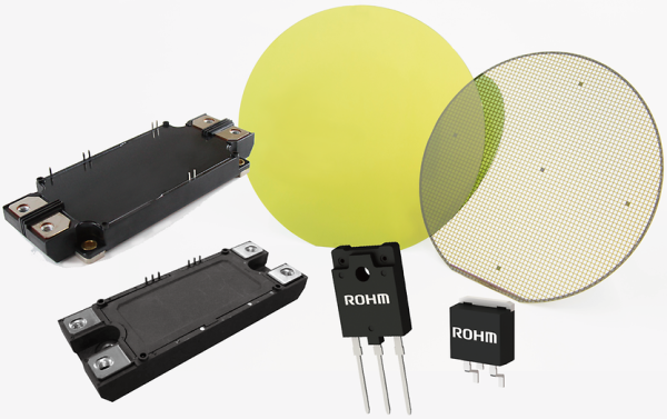
Silicon Carbide (SiC) MOSFETs have emerged as a promising technology to address the increasing demand for high-efficiency and high-frequency power electronics applications. Their unique properties make them superior to traditional silicon-based MOSFETs in several key areas.
SiC properties
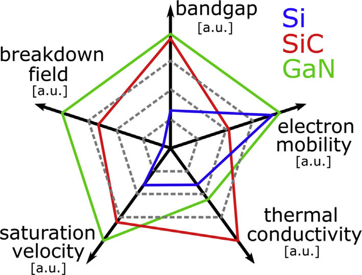
Silicon carbide (SiC) and other wide-bandgap semiconductor materials are increasingly preferred over conventional silicon in many power electronics applications for several key reasons. One of the most important differences lies in the bandgap: SiC typically exhibits a bandgap of about 3.26 electron volts (eV), compared with approximately 1.12 eV for silicon. This wider bandgap allows SiC-based devices to operate reliably at much higher temperatures and voltages, making them particularly suitable for demanding high-power and high-temperature environments.
The main performance advantages of SiC MOSFETs originate directly from the intrinsic properties of the silicon carbide material. Compared with traditional silicon semiconductors, SiC offers superior electrical and physical characteristics that enable improved device operation under harsh conditions. Its wider bandgap supports higher breakdown voltages and elevated operating temperatures, while simultaneously helping reduce both conduction and switching losses, resulting in improved overall energy efficiency.
Another important benefit of SiC is its excellent thermal conductivity, which allows heat to be dissipated more effectively than in silicon-based devices. Efficient thermal management is essential in power electronics systems to ensure reliability and long-term stability, and this characteristic makes SiC especially attractive for compact and lightweight converter designs operating at high power levels.
Electron mobility is another parameter often discussed when evaluating semiconductor performance. Mobility (μ) describes how quickly charge carriers move through a material when subjected to an electric field and is defined as the ratio between carrier drift velocity and the applied electric field (E). Higher mobility is associated with improved electrical conductivity and reduced resistance within the device channel. The maximum achievable carrier velocity is commonly referred to as the saturation drift velocity. These transport properties play an important role in determining switching performance and conduction efficiency in MOSFET structures.
Because SiC devices enable faster carrier transport and benefit from a wider bandgap structure, they support reduced on-resistance (RDS(on)) compared with conventional silicon MOSFETs, particularly at elevated operating temperatures. Lower on-resistance directly translates into reduced conduction losses and improved system-level efficiency, which is especially valuable in high-power conversion applications.
On-resistance is a critical performance parameter in MOSFET devices, strongly influencing both power dissipation and conversion efficiency. Reducing RDS(on) improves current conduction and limits thermal losses, making it a key design objective in applications such as switching power supplies, voltage regulators, and power amplification systems.
In addition to these advantages, SiC offers significantly higher thermal conductivity than silicon—typically around three times greater. This enhanced heat-transfer capability allows SiC devices to operate at higher power densities and within more demanding thermal environments while maintaining reliability and extending operational lifetime.
Another major advantage of SiC technology is its high critical breakdown electric field strength, which can exceed that of silicon by roughly an order of magnitude. This enables devices to support higher voltage ratings without increasing chip size, allowing designers to develop smaller, lighter, and more efficient power conversion systems.
SiC MOSFETs also provide excellent switching performance, characterized by reduced gate charge and faster transition speeds. These features help lower switching losses, particularly in high-frequency operation, and enable higher power density converter architectures. Faster switching combined with reduced conduction losses also results in lower heat generation, simplifying thermal management and supporting more compact, efficient, and robust power electronic system designs.
Specific applications
Silicon carbide (SiC) MOSFETs are used across a wide range of industries, although their strongest adoption today is in electric power systems and power electronics applications. Thanks to their ability to support higher efficiency and increased power density, these devices are widely implemented in modern power converters and inverter architectures. The compact and lightweight systems enabled by SiC MOSFET technology contribute significantly to improving the performance of renewable energy platforms and electric vehicles (EVs), helping extend vehicle driving range while enhancing the efficiency of solar inverters and wind energy conversion systems.
In addition, SiC MOSFETs are particularly well suited for applications requiring high switching frequencies due to their fast switching performance. Higher switching frequencies allow designers to reduce the size of passive components such as inductors and capacitors, enabling more compact converter designs together with improved transient response.
Traction inverters and motor drive systems in electric vehicles also benefit from the higher efficiency and power density made possible by SiC MOSFET technology. Their capability to operate reliably at elevated temperatures makes them especially appropriate for the demanding thermal environments typically encountered in automotive applications, supporting robust and dependable long-term operation.
Beyond traction systems, SiC MOSFETs are increasingly used in electric vehicle charging infrastructure, uninterruptible power supplies (UPS), solar string inverters, and module-level power electronics such as solar optimizers. Their combination of high-voltage capability and improved conversion efficiency continues to drive adoption across next-generation electrification and renewable energy platforms.
SiC MOSFETs are particularly well-suited for a wide range of applications, including:
Automotive: Electric vehicles (EVs) and hybrid electric vehicles (HEVs) require high-efficiency power converters for battery charging, motor drives, and auxiliary power systems. SiC MOSFETs can significantly improve the efficiency and power density of these systems.
Renewable energy: Solar inverters and wind turbine converters benefit from the high efficiency and high-frequency capabilities of SiC MOSFETs, leading to higher energy yields and reduced system costs.
Industrial power supplies: SiC MOSFETs can enhance the efficiency and power density of industrial power supplies, such as those used in data centers and manufacturing facilities.
Consumer electronics: SiC MOSFETs can enable smaller, lighter, and more efficient power adapters and chargers for smartphones, laptops, and other electronic devices.
Challenges and future trends
Although silicon carbide (SiC) MOSFET technology is progressing quickly, several challenges remain, particularly in terms of device cost and long-term reliability optimization. Nevertheless, continuous research and industrial development efforts are steadily addressing these limitations, supporting broader adoption across demanding applications. As manufacturing processes mature and economies of scale improve, SiC MOSFETs are expected to play an increasingly important role in next-generation power electronics systems.
In summary, SiC MOSFETs represent a highly attractive solution for high-efficiency and high-frequency power conversion applications. Their strong electrical performance, thermal robustness, and compatibility with advanced converter architectures position them as a key enabling technology across multiple sectors. With ongoing technological progress and expanding ecosystem support, SiC devices are set to remain central to the evolution of modern electrification and energy-efficient power electronics platforms.
In recent years, planetary exploration missions have achieved significant technological progress, with approximately five robotic rovers successfully deployed on Mars, the most recent being the Perseverance rover. Silicon carbide (SiC) devices are playing an increasingly important role in space exploration, enabling scientists to perform more detailed investigations of planetary surfaces and atmospheres while also supporting future preparation for human missions beyond Earth. Mars is an extremely cold environment, with an average surface temperature of around −70°C. Under such conditions, conventional silicon-on-insulator (SOI) integrated circuit technology can be employed in rover electronic systems. However, these silicon-based ICs typically have a maximum operating temperature near 300°C, beyond which their long-term reliability and performance cannot be maintained.
Venus is considered to be the sister planet of Earth because it has a similar size and composition, and surface exploration of this planet is expected to provide valuable information about Earth’s history. The average temperature on the surface of Venus is about 400°C, which is way above the maximum limit of the functioning of conventional Si-based electronic devices. Previous explorations sent to Venus have proved that these ICs only survived about 2 hours in that environment. This is where SiC devices prove to be powerful candidates. These wide band gap devices are suitable to be used for high-power and high-temperature applications.
FIGURE 1: SILICON CARBIDE-BASED ELECTRONICS
SiC-based devices for space exploration
The atmosphere of Venus is extremely dense and consists primarily of carbon dioxide (about 96.5%), while the planet’s surface temperature reaches approximately 450°C and the atmospheric pressure at the surface is around 92 atmospheres. Earlier Soviet Venus missions, including Venera 7 (1970), which operated for only 23 minutes, and Venera 13 (1982), also demonstrated very limited operational lifetimes because of the planet’s extremely harsh environmental conditions.
Space exploration landers are generally classified into three main categories: short-duration landers, long-duration landers, and mobile surface platforms. Short-duration landers typically operate for only a few hours and are mainly used to perform meteorological measurements and preliminary analysis of surface rocks and soil. Due to their limited mission time, silicon-based electronic devices combined with appropriate cooling strategies can still be used in these systems. In contrast, long-duration landers are designed to function for roughly 120 days and support extended monitoring of environmental parameters such as temperature, pressure, wind speed and direction, atmospheric composition, and seismic activity. Mobile surface platforms, meanwhile, are intended for mineralogical investigations and panoramic imaging of planetary terrain. For both long-duration landers and mobile exploration platforms, conventional silicon electronics are not suitable because silicon loses its semiconductor functionality above about 300°C. As a result, silicon carbide (SiC) technologies are being actively explored as a more reliable alternative for extended missions in extreme environments.
In addition to having a bandgap approximately three times wider than that of silicon (3.2 eV compared with 1.1 eV), silicon carbide is capable of maintaining its semiconductor properties at temperatures approaching 600°C, whereas silicon devices cannot operate reliably beyond roughly 300°C. Owing to this wider bandgap, SiC devices can tolerate higher voltages, greater power densities, stronger radiation exposure, and lower off-state leakage currents compared with conventional silicon components. Furthermore, SiC exhibits excellent thermal conductivity, enabling faster heat dissipation than many other semiconductor materials. This allows SiC power devices to operate at elevated power levels while effectively managing the excess heat generated during operation. In addition, SiC technology offers strong high-voltage blocking capability, reduced on-resistance, and reliable performance at elevated temperatures, supported by a breakdown electric field roughly ten times higher and a thermal conductivity about three times greater than that of silicon.
FIGURE 2: SI V/S SIC V/S GAN
Challenges in SiC-based devices for space exploration
Although silicon carbide (SiC) technology has made significant progress in recent years, it is still less mature than conventional silicon-based manufacturing platforms. Compared with silicon, SiC technology currently faces limitations in wafer diameter availability, fabrication cost, and transistor scaling capability. The channel length of present-day SiC transistors typically remains in the micrometer range, similar to the dimensions achieved by silicon technologies in the 1980s. As a consequence, SiC-based electronics generally operate at lower switching speeds than advanced silicon devices, which restricts their use in highly complex circuits requiring high-frequency performance.
One of the main challenges in SiC fabrication is related to the intrinsic properties of the material itself. Because SiC is extremely hard—approaching diamond-like mechanical characteristics—its crystal growth and processing require higher temperatures, longer processing times, and greater energy consumption than silicon. In addition, the material’s high optical transparency and relatively large refractive index, particularly for the widely used 4H-SiC polytype, make inspection for surface defects more difficult. These limitations can directly influence epitaxial growth quality and ultimately impact device yield.
Typical defects observed during SiC substrate manufacturing include crystalline stacking faults, surface contamination particles, micropipes, pits, scratches, and staining. Studies have indicated that such defects tend to occur more frequently in 150 mm wafers compared with 100 mm substrates, potentially affecting the reliability and performance of SiC-based electronics intended for demanding environments such as space exploration. Furthermore, SiC processing presents additional challenges related to longer production cycle times, higher fabrication costs, and difficulties in wafer dicing, since the material is both extremely hard and relatively brittle. Another limitation arises from the very low diffusion coefficients of dopants in SiC, which makes conventional diffusion-based impurity doping techniques largely impractical.
To address these material and processing constraints, several advanced fabrication approaches have been introduced in recent years. Material-level improvements include both bulk crystal growth and epitaxial layer development, where lightly doped layers with thicknesses typically ranging from about 5 to 100 µm are grown homoepitaxially using chemical vapor deposition (CVD) on off-axis SiC substrates. In parallel, process-level innovations such as ion implantation and in-situ doping during epitaxial growth are now widely adopted as key techniques for the fabrication of SiC power devices.
Conclusion
Beyond planetary missions such as those targeting Venus, many other high-power and high-temperature environments require the development of electronic systems capable of operating reliably under extreme conditions, where silicon carbide (SiC) technology offers clear advantages. Representative application areas include naval propulsion systems, aircraft engine electronics, hybrid and electric vehicles together with their charging infrastructure, railway traction platforms, high-voltage direct current (HVDC) transmission, flexible AC transmission systems (FACTS), photovoltaic energy generation, wind power installations, and smart grid architectures.
To further improve system efficiency while reducing the size and weight of electronic assemblies, SiC is increasingly recognized as a key enabling technology for next-generation power electronics. Recent technological progress indicates that SiC-based solutions are expected to progressively replace conventional silicon devices in many high-power and high-temperature applications over the coming years, supporting more compact, robust, and energy-efficient system designs.
References
[1] H. Kim, J. Bagherzadeh and R. G. Dreslinski, “SiC Processors for Extreme High- Temperature Venus Surface Exploration,” 2022 Design, Automation & Test in Europe Conference & Exhibition (DATE), 2022, pp. 406-411, doi: 10.23919/DATE54114.2022.9774769.
[2] T. Kimoto, “SiC technologies for future energy electronics,” 2010 Symposium on VLSI Technology, 2010, pp. 9-14, doi: 10.1109/VLSIT.2010.5556137.
[3] Friedrichs, Peter. (2007). Technological challenges for manufacturing power devices in SiC. 2007 International Conference on Compound Semiconductor Manufacturing Technology, CS MANTECH 2007.
The introduction of mercury arc valves in the early twentieth century marked a major technological breakthrough because of the wide range of industrial uses they enabled. Later, the emergence of power semiconductor components such as bipolar junction transistors (BJTs) significantly improved efficiency and performance across this market segment, while also helping reduce production costs for power electronic equipment. Over time, semiconductor-based power devices have continued to evolve, and recent progress now includes the integration of artificial intelligence (AI) across the broader power electronics ecosystem.
Today, power electronics plays a central role in nearly all industrial automation environments, supporting both energy generation and transmission processes. Applications such as renewable energy systems, high-voltage direct current (HVDC) transmission, flexible AC transmission networks, electric vehicles, and microgrid infrastructures all rely heavily on semiconductor power technologies. At the same time, ongoing industry transformation is driving the need for more advanced manufacturing techniques, smarter control strategies, and improved maintenance approaches for these devices. Because semiconductor power components typically operate at high switching frequencies, they introduce additional complexity in system control and management. Silicon Carbide (SiC) based JFETs and MOSFETs are one example. Artificial intelligence has proven to be an efficient method of designing, controlling, and sustaining power electrical systems.
AI and Power Electronics
Intelligence is no longer considered an exclusively human attribute. While Industry 3.0 introduced automation into manufacturing environments, it is the emergence of artificial intelligence (AI) and machine learning (ML) that has become a defining element of Industry 4.0. The objective of AI is to allow machines to replicate aspects of human reasoning and decision-making, with the added advantage that these systems can operate continuously without fatigue. Technologies such as facial recognition, autonomous driving systems, speech processing platforms, conversational chatbots, and many other applications are already benefiting from AI-driven capabilities.
Artificial intelligence offers particular advantages in the field of power electronics due to specific operational requirements, including fast parameter tuning and high sensitivity in condition monitoring. In practice, AI can support all three main stages of the power electronics lifecycle: system design, real-time control, and predictive maintenance.
At the same time, the rapid expansion of IoT infrastructures and Big Data analytics platforms has made large volumes of operational data available to train and improve AI models used throughout the lifecycle of power electronic systems.
This growing availability of structured and real-time data is creating strong momentum for the adoption of artificial intelligence within power electronics applications. By leveraging these datasets, AI techniques can enhance product competitiveness through global design optimization, intelligent control strategies, accurate health-state estimation, and other advanced functionalities. As a result, approaching power electronics research from a data-driven perspective is becoming increasingly valuable, particularly in complex and high-performance application scenarios.
AI in Power Electronics: Function and Methods
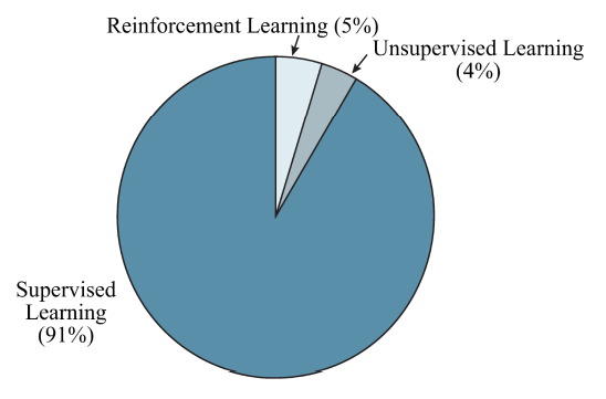
FIGURE 1 SHOWS THE APPLICATION STATISTICS FOR THE ML APPROACH
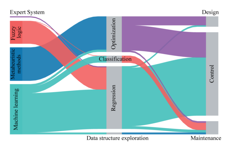
Within the power electronics domain, artificial intelligence is currently applied most extensively during the control stage, followed by maintenance activities, while its adoption in the design phase remains comparatively limited. The main AI functions used in these contexts can generally be grouped into optimization, classification, regression, and data-structure analysis tasks, with regression and optimization representing the majority of practical implementations. Among the most widely adopted artificial intelligence approaches in power electronics are expert systems, fuzzy logic techniques, metaheuristic algorithms, and machine learning methods. In particular, machine learning accounts for a significant share of current applications. For deployment in power electronics environments, ML techniques are typically categorized into supervised learning, unsupervised learning, and reinforcement learning.
At present, expert systems and fuzzy logic are applied less frequently—especially fuzzy logic approaches—but the increasing availability of more powerful computing platforms is enabling the adoption of increasingly advanced AI-based solutions. Metaheuristic optimization methods are also widely used in power electronics and continue to evolve over time. These techniques can operate either as standalone tools or in combination with machine learning algorithms to address complex optimization challenges. More recently, reinforcement learning (RL) has emerged as one of the most promising frontiers in machine learning for power electronics, supported by rapid progress in computing capabilities and processing performance.
FIGURE 2: SANKEY DIAGRAM ILLUSTRATING AI METHODOLOGIES AND APPLICATIONS IN EACH PHASE OF THE POWER ELECTRONIC SYSTEM LIFE-CYCLE.
AI’s potential in power electronics in the future
Despite extensive literature review and study on the potential application of AI in power electronics, it has yet to realize its full potential. Training AI models for deeper improved optimization requires deeper research and analysis.
There are various reasons why industries are hesitant to use AI. Some examples are:
1) Implementation complexity
2) Concerns about algorithm reliability and accuracy
3) Additional hardware costs
4) Significant computational energy usage
Another major challenge affecting the adoption of artificial intelligence in power electronics is the limited availability of large, high-quality datasets required for effective model training. Generating these datasets is often time-consuming, and the amount of data accessible for safety-critical applications is even more restricted. For this reason, there is a growing need to develop data-efficient AI approaches capable of delivering reliable performance even when only small training datasets are available.
Equally important is the development of transparent and interpretable AI algorithms that can increase confidence among engineers and industry professionals working in safety-sensitive environments. A clearer understanding of how these models operate enables designers to refine their behavior and adapt them more effectively to specific application requirements. As Industry 4.0 continues to advance toward highly autonomous and connected smart factories, artificial intelligence and machine learning are becoming central enabling technologies. Power electronics and AI together represent two highly influential technological domains with the potential to drive major industrial transformation. Although several challenges still need to be addressed to fully integrate AI into power electronics systems, continued research efforts are making this objective increasingly achievable.