



Power electronics applications, especially those requiring high efficiency, are increasingly moving away from conventional silicon-based components toward wide-bandgap (WBG) materials. Among these developments, the Gallium Nitride (GaN) bidirectional switch (BDS) is considered one of the most transformative technologies.
Several power topologies, such as electric vehicle (EV) onboard chargers (OBCs) and renewable energy inverters, require bidirectional current flow. In many cases, however, the industry has relied on simple workarounds based on unidirectional components. The advent of monolithic GaN BDS solutions is a major advancement that has overcome these legacy limits, enabling designers to achieve higher power densities and efficiency.
Bidirectional architecture
In conventional power systems, the use of two separate MOSFETs or IGBTs in a back-to-back configuration (typically in common-source or common-drain configuration) is the standard practice for bidirectional operation.
This configuration is needed because normal power transistors are inherently unidirectional. In fact, due to their internal body diodes, they cannot block voltage in either direction.
While this method can work effectively, it occupies more physical space and is inefficient electrically. When the number of electronic components doubles, the conduction losses also double because the current must pass through two transistors, and the footprint on the printed circuit board (PCB) increases.
The problem is easier with GaN technology due to a structural advantage. Because GaN High-Electron-Mobility Transistors (HEMTs) are lateral devices, they lack the inherent parasitic body diode of vertical silicon MOSFETs.
This lateral nature allows the engineer to design a monolithic bidirectional switch on a single die. A monolithic GaN BDS typically consists of two gates and one drift region. The architecture enables the device to block voltage and conduct current in both directions, with a single device, replacing two separate transistors and their packaging [1].
Leading chipmakers innovations
Recent developments in the electronics industry have underscored the need to adopt this technology.
Infineon Technologies, for instance, has introduced the CoolGaN 650 V G5 BDS [2], which represents a significant step toward highly integrated components. This device is designed to replace traditional back-to-back switches for applications such as motor drives and battery control systems.
Infineon’s GaN BDS integrates two gates into a single GaN HEMT structure. This solution demonstrates that it is possible to achieve significantly lower on-state resistance (RDS(on)) than with two discrete devices in series, as current flows through only one channel and one set of contact resistances.
The symbol for the CoolGaN BDS 650 V G5 is shown in Figure 1. The BDS is a five-terminal device, consisting of two gates (G1, G2), two sources (S1, S2), and one substrate terminal (sub).
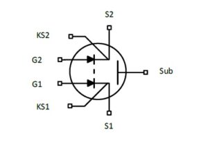
The BDS modes of operation are summarized in the following table.
| G1 | G2 | Modes |
| OFF | OFF | Bidirectional OFF (switch mode OFF) |
| ON | ON | Bidirectional ON (switch mode ON) |
| ON | OFF | Reverse blocking (diode mode RB) |
| OFF | ON | Forward blocking (diode mode FB) |
The Fraunhofer Institute for Applied Solid State Physics (IAF) has unveiled a 1,200 V GaN bidirectional switch that further extends the voltage boundary [3]. The 1,200 V GaN BDS (Figure 2), built using the proprietary GaN-on-insulator technology, includes two free-wheeling diodes and maintains a compact form factor, proving that monolithic bidirectionality is not limited to low-voltage consumer electronics.
This development is particularly relevant for future power systems, such as 800 V EV architectures and industrial grid-tied inverters, where higher voltage margins are critical for reliability and safety.

Renesas Electronics has also entered this technology with a 650 V bidirectional GaN switch that focuses on ease of integration. Their approach accentuates reducing parasitic inductance, a common bottleneck in high-speed switching applications.
By eliminating the interconnects required between two discrete, back-to-back devices, these monolithic solutions minimize loop inductance, which often leads to voltage ringing and electromagnetic interference (EMI). This makes it easier for engineers to design stable, high-frequency converters that fully leverage GaN’s inherent switching speeds.
Renesas’ TP65B110HRU is a 650V, 110 mΩ, high-voltage GaN bidirectional switch capable of blocking both positive and negative currents with a single device (Figure 3).
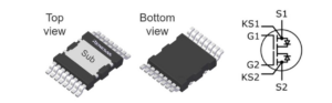
The BDS integrates a monolithic, bidirectional, high-voltage, depletion-mode GaN with normally-off, low-voltage silicon MOSFETs. It provides a high threshold for standard gate-drive compatibility, easy integration, and robust reliability. By enabling single-stage power conversion, this device requires fewer components and achieves higher efficiency than traditional unidirectional silicon (Si) or SiC switches.
Navitas Semiconductor has introduced 650 V bidirectional GaN power ICs, paired with a dual-channel isolated GaN driver. These Bi-Directional GaNFast power ICs function as two back-to-back GaN power switches, featuring a monolithic, single-chip design with a merged drain structure, two gate controls, and a patented, integrated, autonomous substrate clamp.
One of the most significant advantages of this technology is its component consolidation. A single high-speed, high-efficiency bidirectional GaNFast IC replaces up to four older switches, delivering over a 50% reduction in PCB footprint, more than 20 times lower gate charge (QG), and 10 times lower output capacitance (COSS). This translates directly into higher reliability, simplified circuit design, and reduced system cost.
A key enabler of stable and efficient operation is the active substrate clamp. Navitas’ patented monolithically integrated active substrate clamp automatically connects the substrate to the source terminal with the lowest voltage potential, eliminating the back-gating effect, achieving up to 3× lower resistance, and operating approximately 15°C cooler.
Target applications include EV on-board charging, roadside EV charging, solar microinverters, energy storage, and motor drives. The portfolio currently includes the NV6428 and NV6427 devices, both rated at 650 V continuous and 800 V dynamic, and available now in the TOLT package.
Efficiency and thermal management
The primary driver for adopting monolithic BDS technology is the significant improvement in conversion efficiency. In a standard back-to-back silicon MOSFET configuration, the total conduction loss equals the sum of the RDS(on) values of both devices.
In contrast, a monolithic GaN BDS reduces this path to a single device channel. Furthermore, GaN’s superior electron mobility enables lower RDS(on) for a given die size than silicon. This reduction in conduction loss directly translates into less heat generation, a critical factor in high-power applications.
Thermal management is further simplified by the reduced component count. A single monolithic BDS occupies roughly half the space of a back-to-back pair, enabling more localized, efficient cooling strategies. This “scaling down” of the power stage enables the design of smaller, lighter enclosures, which is a major requirement in the automotive and aerospace sectors, where every gram of weight impacts overall system range and performance.
Applications
The benefits of monolithic BDS are most evident in specific power topologies, such as the buck-boost converter and the matrix converter. In a buck-boost configuration for battery charging and discharging, a GaN-based BDS can handle bidirectional energy flow between the battery and the DC bus with fewer components and at higher switching frequencies. Higher frequencies enable the use of smaller inductors and capacitors, additionally reducing the size and cost of the total system.
Matrix converters, which provide direct AC-to-AC conversion without a bulky DC-link capacitor, stand to gain the most from this technology. Traditionally, matrix converters have been limited by the intricacy and losses associated with the large number of bidirectional switches required.
By replacing the complex back-to-back discrete assemblies with monolithic GaN BDS units, designers can finally realize the potential of matrix converters in motor drives and renewable energy interfaces, achieving high power density and sinusoidal input/output currents with minimal harmonic distortion.
Furthermore, integrating these switches into solid-state circuit breakers (SSCBs) remains an active area of research. Unlike mechanical breakers, SSCBs with GaN BDS can interrupt fault currents in microseconds. Bidirectional capability is essential for AC grid applications, where fault current can flow in either direction, depending on the nature of the transient event.
Future outlook
The future of power systems depends on the ability to manage energy more flexibly and efficiently. Monolithic GaN bidirectional switches address the inherent limitations of silicon by offering a streamlined, high-performance alternative to the status quo.
By reducing conduction losses, minimizing parasitic inductances, and drastically shrinking the power stage’s physical footprint, these devices are setting a new standard for electrical engineering.
Whether in the context of next-generation electric vehicles or the modernization of the electrical grid, the transition to GaN BDS technology marks a critical milestone in the pursuit of sustainable, efficient power conversion.
References
[1] V. Veliadis, T.M. Jahns, “Monolithic Bidirectional Lateral GaN Switches Reinvigorate Power Electronics Applications.”
[2] Infineon Technologies AG, “CoolGaN Bidirectional Switch 650 V G5: Fundamentals and design considerations.”
[3] Fraunhofer IAF Press Release, “Bidirectional 1200 V GaN switch with integrated free-wheeling diodes.”
