Schneider Electric’s White Paper 219 is one of the first comprehensive engineering analyzes of arc flash hazards in emerging 800 VDC AI data center architectures. The authors show that, unlike DC systems which are just an extension of traditional AC installations, converter-fed 800 VDC networks require an architecture-aware approach, where the fault characteristics are dominated by transient behavior, converter control and energy storage.
A major strength of the paper is its realistic system modeling. The traditional NFPA 70E methods are still useful as conservative screening tools, but the authors clearly show that the simplified calculations tend to over-estimate incident energy because they assume steady-state fault currents. The use of MATLAB/Simulink transient simulation and ETAP analysis provides a much more accurate representation of capacitor discharge, converter current limiting and protection timing. The rack-level vs centralized debate is a great example of the fact that safety is defined by topology – not just operating voltage.
The paper also reinforces an important message for AI infrastructure designers: 800 VDC is not inherently more dangerous than AC. The case studies demonstrate incident energy below commonly accepted PPE thresholds with current-limited converters, reverse current blocking, and proper coordination of protection. The finding debunks popular myths about high-voltage DC distribution and accelerates the industry’s transition to more efficient AI power architectures.
However, interesting opportunities from a GaN point of view are not explored in the paper. The analysis focuses on the converter-controlled behavior, but the semiconductor technology on which these converters is based is missing. Gallium Nitride (GaN) power devices offer significant improvements to the discussion thru their ultra-fast switching speed, low output capacitance and excellent current-limiting capability, naturally lending themselves to architectures that minimize fault energy. Modern GaN converters are able to isolate faults in a microsecond and reduce the stored magnetic and capacitive energy in comparison to conventional silicon solutions. These features are directly supportive of the findings of the paper that transient duration and not only peak current is the main parameter controlling the arc flash severity.
Future revisions could therefore include comparisons between silicon, SiC and GaN converter implementations. Such analysis would provide quantification of the impact of semiconductor technology on fault waveforms, capacitor sizing, converter response time and ultimately incident energy. Similarly, as a complement to the protection strategies mentioned during the study, emerging GaN-based solid-state circuit breakers could be assessed.
An additional valuable addition would be experimental validation with commercial 800 VDC GaN power platforms. Real measurements of converter turn off dynamics, reverse current blocking capability and fault interruption would increase confidence in the use of simulation-based methodologies.
This white paper is an important contribution to the industry’s understanding of DC arc flash in AI data centers overall. Its focus on architecture provides a solid basis for the future development of standards. A wider perspective, including the role of wide-bandgap semiconductors, and in particular GaN, would make the work even more relevant as AI infrastructure increasingly adopts high-density, high-efficiency power conversion technologies.
Power Integrations has announced an expansion of its PowiGaN™ gallium-nitride (GaN) technology platform to a 2200 V voltage rating, establishing what the company identifies as the highest voltage capability among commercially available GaN solutions. The development targets high-voltage applications across data center, electric vehicle, renewable energy, and high-voltage direct current (HVDC) infrastructure segments.
The advancement addresses a growing industry requirement for higher-voltage bus architectures as power systems seek improved density without sacrificing efficiency. While GaN-based power switches have increasingly displaced silicon transistors in power conversion applications—owing to superior efficiency and higher switching frequencies—existing GaN technology has faced voltage ceilings that limit its applicability in next-generation high-power infrastructure roadmaps.
Historically, designers seeking to accommodate higher-voltage requirements have relied on two primary alternatives: silicon carbide (SiC) devices, which typically operate at lower switching frequencies, or configurations of stacked, lower-voltage GaN components. Both approaches introduce trade-offs, including reduced power density, increased design complexity, and potential reliability concerns associated with multi-device stacking architectures.
Power Integrations’ existing PowiGaN portfolio already includes 1700 V-rated ICs deployed in single-stage auxiliary power applications for data centers, alongside 1250 V devices used as an alternative to stacked configurations within the main power path of 800 VDC data center architectures. The newly introduced 2200 V rating extends this capability further, enabling support for higher-voltage bus designs while avoiding the architectural compromises associated with stacked or SiC-based alternatives.
According to the company, this higher voltage rating is intended to support power system designs not only within data center infrastructure but also across electric vehicle powertrains, photovoltaic inverter systems, and battery energy storage applications—sectors where increasing power density and voltage headroom are becoming central design considerations. By extending GaN’s voltage ceiling, Power Integrations positions PowiGaN as a scalable solution capable of addressing near-term and future infrastructure requirements without necessitating a shift to alternative semiconductor technologies or more complex circuit topologies.
Schneider Electric has published a first-of-its-kind technical analysis examining arc flash risk within 800 VDC power architectures, offering data-driven guidance for facilities transitioning to this emerging distribution standard for AI-oriented data centers.
The study, developed in alignment with design patterns used by major hyperscale operators, evaluates two representative 800 VDC configurations under varying conditions. Results indicate that arc flash severity is primarily a function of system architecture, capacitor placement, and fault-clearing timing rather than an inherent characteristic of DC distribution itself. Notably, even under conservative, capacitor-dominated fault assumptions, the analysis found that arc flash exposure in 800 VDC systems can be kept within manageable limits, often comparable to conventional AC installations.
This research addresses a timely gap: while arc flash assessment is well-established practice for AC data center environments, no unified industry standard currently governs electrical hazard evaluation for converter-fed 800 VDC systems. As rack densities climb toward 400 kW and beyond, driven largely by NVIDIA-led initiatives and supporting infrastructure partners including Schneider Electric, understanding fault behavior and protection coordination at these voltage levels becomes increasingly critical.
Two architecture types were assessed. The rack-level, or “sidecar,” configuration produced incident energy levels well under the 1.2 cal/cm² PPE reference threshold, even in scenarios lacking dedicated protection devices. The centralized, facility-level architecture showed a potential for marginally higher incident energy under worst-case, unprotected conditions; however, results varied depending on fault location relative to reverse-blocking diodes, which influence back-feed current and peak fault behavior. When standard time-based protection devices were applied, incident energy dropped to levels broadly consistent with typical AC systems.
Key findings emphasize that arc flash events in 800 VDC systems are governed by transient, time-dependent fault currents, with capacitor discharge dominant in the earliest milliseconds. The study also found that conventional arc flash calculation methods tend to overstate risk in capacitor-heavy systems, and that simulation-based tools, such as ETAP’s transient modeling and digital twin capabilities, offer more accurate risk characterization. Ultimately, careful attention to capacitor placement, protective device selection, and millisecond-scale fault clearing emerged as the primary levers for managing safety outcomes.
I was in Shanghai on June 30 for Infineon’s 2026 Media Day, held at the company’s Greater China headquarters in Zhangjiang under the theme “From Innovation to Value.” Infineon’s Greater China leadership — including David Poon, global senior vice president and Greater China president, and Cao Yanfei, senior vice president and head of the automotive business in Greater China — walked the room through the company’s overall strategy and localization plan, then through the automotive, industrial and infrastructure, and consumer, computing and communications businesses in turn. A few years ago, the power discussion around AI infrastructure could still be overshadowed by the GPU discussion. That is getting harder.
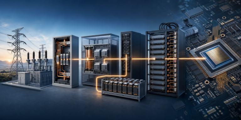
Infineon framed the AI data center problem from a different starting point: not the processor, not the rack, and not the power supply unit alone, but the full route from grid connection to processor core. The company called it a “From Grid to Core” view, and the framing matters because rack power is moving fast. The event materials described a shift from roughly 200 kW-class AI racks to about 500 kW today, with the next generation potentially moving toward 1 MW.
If that trajectory holds, power semiconductors move from supporting hardware to shaping the architecture around it.
The rack is pulling the power chain into one conversation
Infineon’s media-day message was built around one practical issue: AI compute density is rising faster than legacy power architectures were designed to absorb. A 500 kW or 1 MW rack changes the stress on every conversion stage — solid-state transformer (SST), uninterruptible power supply (UPS), battery backup unit (BBU), power supply unit (PSU), intermediate bus converter (IBC), voltage regulation module (VRM), and the final CPU/GPU power stage — well beyond simply carrying a larger load. Infineon’s public event release described a full-chain solution covering generation, transmission and distribution, storage, data center infrastructure, and physical AI applications such as EVs and robotics.
The more technical version is sharper: each conversion stage now becomes part of the AI performance envelope. That is why “grid to core” serves as a design principle: energy loss, dynamic response, footprint, thermal stress, and redundancy now need to be jointly optimized across every conversion stage. Cheng Jiayu, Senior Vice President of Infineon Technologies and Head of Industrial & Infrastructure Business Greater China.
Infineon’s restructuring turns portfolio breadth into a system argument
The company’s recent restructuring also points in this direction. From July 1, 2026, Infineon moved from four divisions to three: Automotive, Power Systems and Edge Systems. The official Media Day release positioned the change as a way to improve agility and accelerate system-level innovation.
For power customers, the logic is fairly direct. A data center power chain may use silicon MOSFETs, SiC, GaN, drivers, controllers, sensors, and protection devices in a single design. A customer buys efficiency, density, reliability, a stable supply, and a shorter development cycle, with the internal product-line map remaining invisible to them.
This is where Infineon is trying to turn portfolio breadth into a system argument. Cao Yanfei, Senior Vice President of Infineon Technologies and Head of Automotive Business Greater China. Source: Infineon.
The same pattern shows up outside AI data centers. In 2025, Infineon completed the acquisition of Marvell’s Automotive Ethernet business, strengthening its position in software-defined vehicles and adding high-bandwidth in-vehicle networking capability. In 2026, it announced the acquisition of ams OSRAM’s non-optical analog/mixed-signal sensor portfolio, adding sensor assets for automotive, industrial and medical markets.
On their own, these moves keep Infineon outside the data center business. Together, they point in the same direction of travel: control, power, sensing, connectivity, and safety are being integrated at the system level.
SiC and GaN are becoming placement decisions
The event also positioned the wide-bandgap discussion beyond a simple SiC-versus-GaN debate, a framing that matches how the two technologies are actually deployed. SiC is more naturally positioned in high-voltage, high-power, high-reliability stages: SST, DC microgrids, UPS and large front-end conversion. GaN is more compelling where high switching frequency, compact magnetics and high power density matter: data center PSUs, IBCs, robotics, solar inverters and onboard charging.
Silicon remains part of the stack because cost, maturity and scale still matter. Infineon has been explicit about this materials strategy. In 2024, the company announced 300 mm power GaN wafer technology, using existing 300 mm silicon manufacturing infrastructure as part of its longer-term GaN scaling roadmap.
At the same time, the company continues to position SiC as a key technology for high-efficiency energy conversion and power infrastructure. For system architects, the decision comes down to placement: where each material sits at the right voltage, frequency, thermal and reliability boundary.
China is becoming part of product definition
The other important thread from the Shanghai event was localization. Infineon’s “In China, for China” strategy is often easy to read as manufacturing localization. The Media Day suggested a broader shift: local production, local quality systems, local product definition, local innovation platforms and local operating infrastructure.
The production roadmap included 40 V MOSFET localization, 40 nm AURIX TC3x and 28 nm automotive radar sensor front-end and back-end localization plans, and DSO packaging scale-up for analog/mixed-signal products. The company also highlighted reliability testing and failure analysis capability in Wuxi, Shanghai Innovation Space, a robotics lab in Hong Kong, 19 innovation application centers, six system competence centers, and additional application labs. The strategic implication is straightforward.
China is becoming a place where product definition, system validation, and application learning occur earlier, extending its role well beyond that of an end market for power semiconductors. That matters for AI power, EVs, robotics and energy infrastructure because these markets are moving with local system requirements, local cost pressure and fast iteration cycles.
The capacity question is really an allocation question
David Poon, Senior Vice President of Infineon Technologies and President of Greater China. Source: Infineon. Infineon also linked AI data center demand to supply capability.
The company discussed its €5 billion smart power semiconductor fab in Dresden, scheduled to begin operation on July 2, and an additional €500 million investment in fiscal 2026 to expand capacity. It also referred to a “One Virtual Fab” model to improve supply-chain resilience and customer response. The AI numbers explain why this matters.
Infineon has publicly projected €2.5 billion in AI market revenue for fiscal 2027, supported by its position across the AI power delivery chain. The harder issue lies in allocation: how an IDM simultaneously allocates high-reliability power capacity among AI data centers, automotive, industrial infrastructure, and energy systems. Automotive and industrial customers care about long-term supply assurance, qualification stability, and quality consistency.
AI infrastructure is creating a faster growth curve. The tension is manageable only if manufacturing, portfolio planning, and customer engagement are treated as a single system.
Power semiconductor competition is moving up the stack
The most important message from Infineon’s 2026 Media Day was structural. Infineon connected automotive semiconductors, power devices, MCUs, sensors, Ethernet, SiC, GaN, data center power and China localization under one operating logic: system-level capability. For the next phase of power semiconductor competition, device parameters still matter.
Cost still matters. Supply still matters. But the differentiation is moving higher in the stack.
The companies that win the next AI power cycle may be the ones that can participate earlier in system definition, combine multiple semiconductor technologies into a single architecture, localize quickly enough for regional customers, and still guarantee reliability across long product lifecycles. Infineon’s bet is that “grid to core” marks the direction in which power semiconductor value is moving, extending well beyond a single data center story. Having sat through the full media-day agenda, I’d treat the three-division restructuring and the Dresden capacity build-out as the two signals worth watching over the next few quarters — they will show whether “grid to core” becomes an operating structure or remains a slogan.
Sources
[1] Infineon 2026 Media Day: Innovation Space officially opened Infineon / PR Newswire Asia, June 30, 2026
[2] Infineon successfully completes acquisition of Marvell’s Automotive Ethernet business, Infineon, August 14, 2025
[3] Infineon acquires non-optical analog/mixed-signal sensor portfolio from ams OSRAM, Infineon, February 3, 2026
[4] Infineon pioneers 300 mm power GaN technology, Infineon, September 11, 2024
[5] Infineon named as the Company to Beat in AI Data Center Power Semiconductors by Gartner, Infineon, June 26, 2026
Traditional space LDOs rely on silicon MOSFETs that suffer from radiation degradation. To solve this, Tony Marini from EPC Space highlights a revolutionary alternative using enhancement-mode Gallium Nitride (eGaN) HEMTs. Their unique material physics inherently resists Total Ionizing Dose (TID) effects without performance loss, ensuring exceptional parameter stability in harsh orbital environments.
GaN Physics and Radiation Mitigation Mechanisms
Unlike silicon MOSFETs, which rely on physical oxide interfaces that trap positive charges when exposed to low-dose ionizing radiation (<30 kRad), eGaN HEMTs feature a wide bandgap structure devoid of such vulnerable gate oxides. In silicon devices, this trapped charge reduces the transconductance (gm) by 20% or more, forcing the analog voltage control loop to constantly adjust over wide operating margins to maintain regulation.
In contrast, Tony Marini emphasizes that eGaN HEMTs are virtually immune to low-dose radiation. The transconductance—defined in Siemens as the ratio of change in drain current to the change in gate-source voltage (ΔId /ΔVgs)—exhibits a typical decrease of less than 3% under equivalent low-dose exposure. Because gm closely follows the gate-source threshold voltage (Vgs(th)) performance, this physical resilience prevents the regulator’s analog control loop from “hunting” across a broad voltage range to achieve stable output regulation.
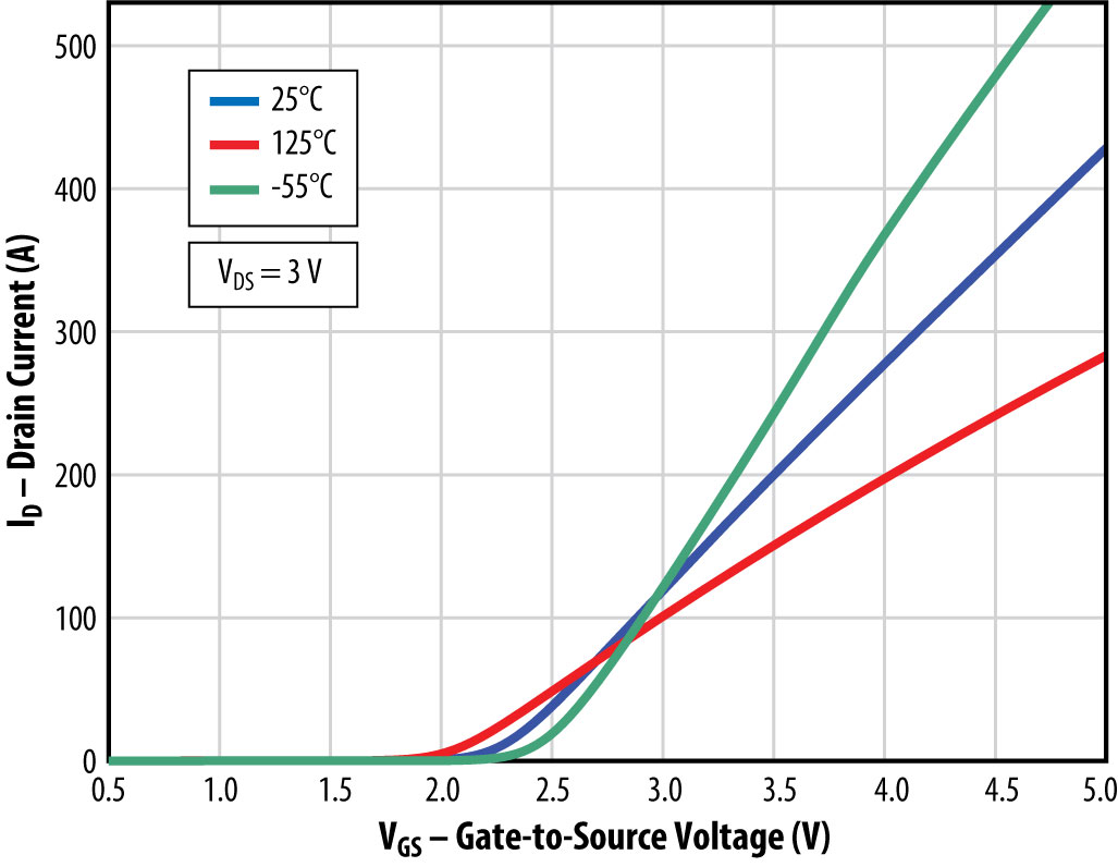
The typical transfer characteristics (Figure 1) that define the stability of these systems are anchored in the specific behavior of the pass elements under distinct temperatures and biasing configurations, as detailed in the technical data provided by EPC Space.
Figure 1: Typical transconductance curve (Id vs.Vgs) for the EPC7019G (40 V/90 A) pass element utilized in high-current linear regulation architectures.
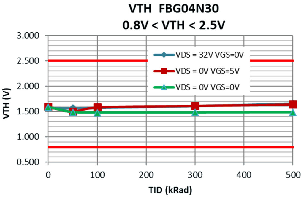
Furthermore, experimental evaluation demonstrates that the threshold voltage (Vth) remains remarkably flat across extensive Total Ionizing Dose (TID) testing profiles. Figure 2 illustrates the robust operational envelope of a representative eGaN HEMT device (such as the FBG04N30 platform) under continuous exposure up to 500 kRad.
Figure 2: Total Ionizing Dose (TID) performance displaying the high stability of Vgs(th) up to 500 kRad for GaN technology.
Gate Biasing Challenges and Structural Implementation
Because eGaN HEMTs are exclusively available as n-channel polarity devices, implementing them as pass elements introduces specific biasing constraints. To maintain proper linear regulation, the bias potential provided to the gate terminal must remain slightly higher than the combined magnitude of the output voltage and the maximum gate-source voltage required at full load current:
Vbias > Vout + Vgs (Id(max))
According to the insights shared by Marini, the exceptional stability of Vgs against aging, temperature swings, and radiation allows designers to set the required gate bias potential as low as possible. For instance, in a system configured for a regulated 5.0 Vdc output, a stable gate bias potential of approximately 8.5 V (relative to the circuit’s ground return) can be safely utilized. This tight tolerance window minimizes overhead power consumption and safeguards the error amplifier stage from unnecessary voltage stresses.
Evaluation Boards Architecture & Interface
Implementing eGaN HEMTs as pass elements in linear regulation architectures requires a detailed analysis of their circuit environment and control interfaces. EPC Space designed two evaluation platforms, designated as the EPC7C023 (optimized for an operating regime up to 5 A) and the EPC7C024 (designed for an operating regime up to 0.5 A). The purpose of these boards is to serve as test vehicles to isolate and study the physical behavior of GaN devices operating within the linear region.
Control Loop Topology and Semiconductor Selection
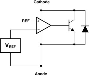
To prevent complex compensation networks from introducing additional variables into the semiconductor’s analysis, a fundamental analog control loop was implemented based on the TL1431 integrated circuit. This component operates as a shunt regulator that integrates both the error amplifier and an internal bandgap voltage reference onto a single silicon die, whose internal topology is detailed in the block diagram of Figure 3.
Figure 3: TL1431 IC Controller Simplified Block Diagram (Source: TI).
The differentiation in current conduction capacity between the two platforms relies exclusively on the sizing of the eGaN HEMT used as the power pass element (Qpass):
High-Current Platform (EPC7C023): Integrates the EPC7019G device, characterized by a maximum voltage rating of 40 V, a current capacity of 90 A, and a fully-enhanced drain-source on-resistance (Rds(on)) of 4.5 mΩ.
Low-Current Platform (EPC7C024): Employs the EPC7014UB device, dimensioned for lower-magnitude analog precision loads.
Tony Marini emphasizes that the pass transistor never operates in a fully-enhanced state during active regulation. If the HEMT turned on completely, it would act as a closed switch and lose its ability to modulate drain current via gate-source voltage, causing the control loop to lose regulation. Therefore, the nominal Rds(on) of 4.5 mΩ serves only as an asymptotic limit to approximate resistance at the saturation boundary and estimate the minimum dropout voltage.
Analytical Modeling of Dropout Voltage and Parasitic Variables
The theoretical minimum dropout voltage (Vdo(min)) of this architecture is determined by summing the ohmic losses across the partially enhanced semiconductor channel and the voltage drop across the series-connected current sense resistor (Rcs):
Vdo(min) ≅ Iout . (Rds(on_sat) + Rcs)
Applying the specific parameters of the EPC7C023 board under a maximum load of 5 A yields the following initial calculation:
Approximate drop across the HEMT (EPC7019G): ≅5 mV.
Drop across the sense resistor (Rcs = 10 mΩ): 50 mV.
Theoretical lower dropout limit: 72.5 mV.
Physical characterization of the circuit on the test bench revealed an actual measured dropout voltage of 152 mV, representing a deviation from the simplified mathematical model. Marini explains that this increase stems from real-world physical factors in thermal and geometric modeling: primarily the distributed parasitic resistance within the PCB copper traces (PCB copper etch resistance) and the fact that the EPC7019G HEMT enters hard saturation at a slightly lower Vgs potential than theoretically estimated under static linear biasing conditions.
Layout Thermodynamics and Parasitic Suppression on the PCB
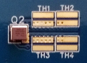
To manage continuous linear power dissipation (PD = (Vin – Vout) . Iout) without bulky heatsinks, the PCB utilizes planar Vishay ThermaWick aluminum nitride (AlN) components (designated as TH1–TH4 in Figure 4). Four elements are populated on the 5 A board (EPC7C023) for lateral heat routing, while none are required on the 0.5 A variant (EPC7C024).
Figure 4: ThermaWick “Helper” Elements on the EPC7C023 and 7C024 Eval. Boards.
Regarding signal integrity and stability against high-frequency transients, the presence of parasitic inductances and capacitances poses a risk of oscillation at the control (gate) node. The implemented physical countermeasure consists of minimizing current loop areas by routing the power lines connected to the drain and source of the pass element with copper traces that are as short and wide as possible, reducing both DC resistance and electromagnetic noise coupling.
Monitoring Interface Configuration and Transfer Equation
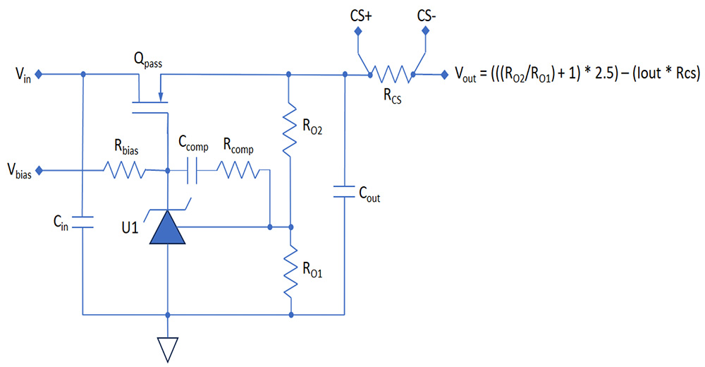
Each board exposes six power terminals (Vin±, Vout±, VBIAS±) and high-impedance differential pads (CS+/CS-). To isolate the native GaN dropout, the sense resistor (Rcs = 10 mΩ for EPC7C023; 50 mΩ for EPC7C024) sits outside the feedback loop. No dedicated enable pin exists; dropping Vbias to 0 V serves as the turn-off mechanism.
The electrical coupling of all these variables is consolidated in the circuit schematic analyzed in Figure 5. The regulated output voltage (Vout) follows:
Vout = ((Ro2/Ro1) + 1) . 2.5 V – (Iout . Rcs)
Figure 5: EPC7C023 and 7C024 Eval. Boards Simplified Schematics.
Performance Verification & Test Results
Control Loop Simulation and Stability Analysis
Prior to finalizing the bill of materials (BOM) for the evaluation boards, Tony Marini notes that the control loop’s voltage regulation performance was verified via LTSPICE numerical simulation. To validate stability without early overhead, the implementation utilized a standard, historical simulation model of the TL1431 IC controller acting as the analog error amplifier and bandgap reference.
Instead of validating loop margins via standard frequency-domain Bode plots, Marini utilized the time-domain load transient response to prove system stability. The loop compensation architecture, using a simple parallel resistor-capacitor network, was kept as unadorned as possible. This minimalist baseline prevented external compensation parameters from masking the raw, intrinsic performance of the eGaN HEMT pass transistor.
Load Transient Response Verification
The physical transient verification proved that both platforms exhibit fast recovery windows and remain entirely free of control loop oscillations across their maximum step-change boundaries.
Metric
EPC7C023 (5 A Version)
EPC7C024 (0.5 A Version)
Output Current Step Range
100 mA to 5 A
10 mA to 500 mA
Peak Voltage Deviation Amplitude
~160 mV
~110 mV
Response / Recovery Time
~50 µs
~40 µs
High-Current Subsystem (EPC7C023) Performance
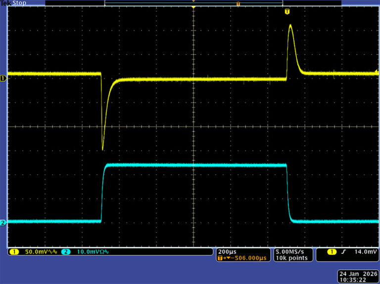
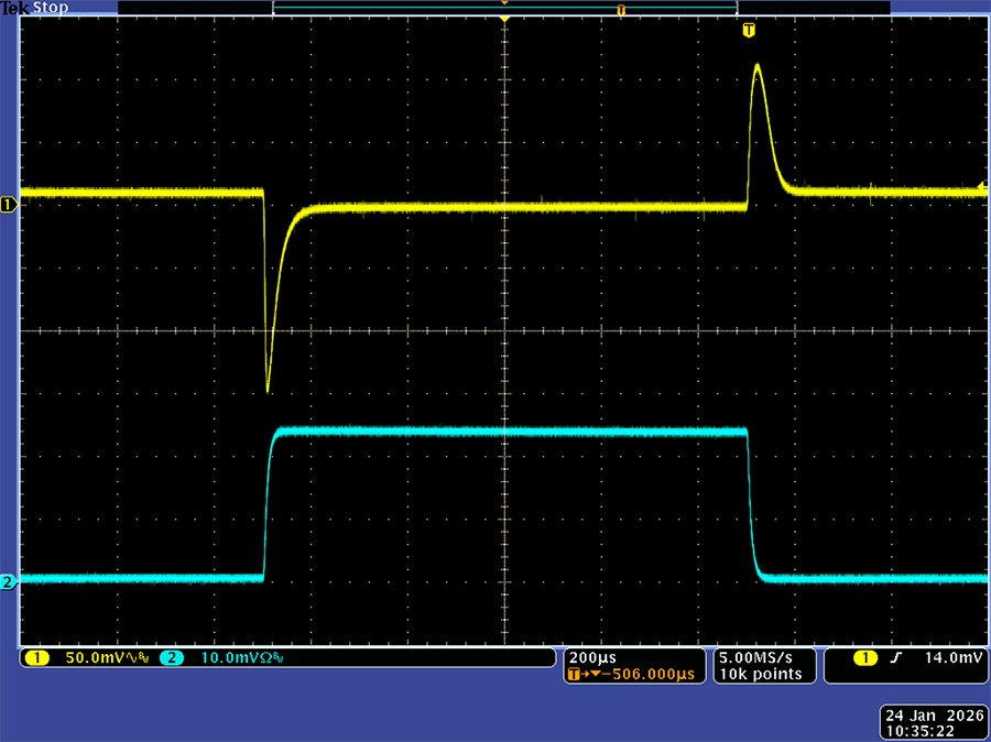
For the large-die HEMT configuration (EPC7019G), the load current was stepped across virtually its full operating range, spanning from 0.1 A to 5 A. As captured in the hardware test data below (Figure 6), the control loop dampens the step transition within ~50 µs, maintaining a tight peak voltage deviation of only ~160 mV.
Figure 6: EPC7C023 Current Step-Change Response: 0.1A-to-5A.
Low-Current Subsystem (EPC7C024) Performance
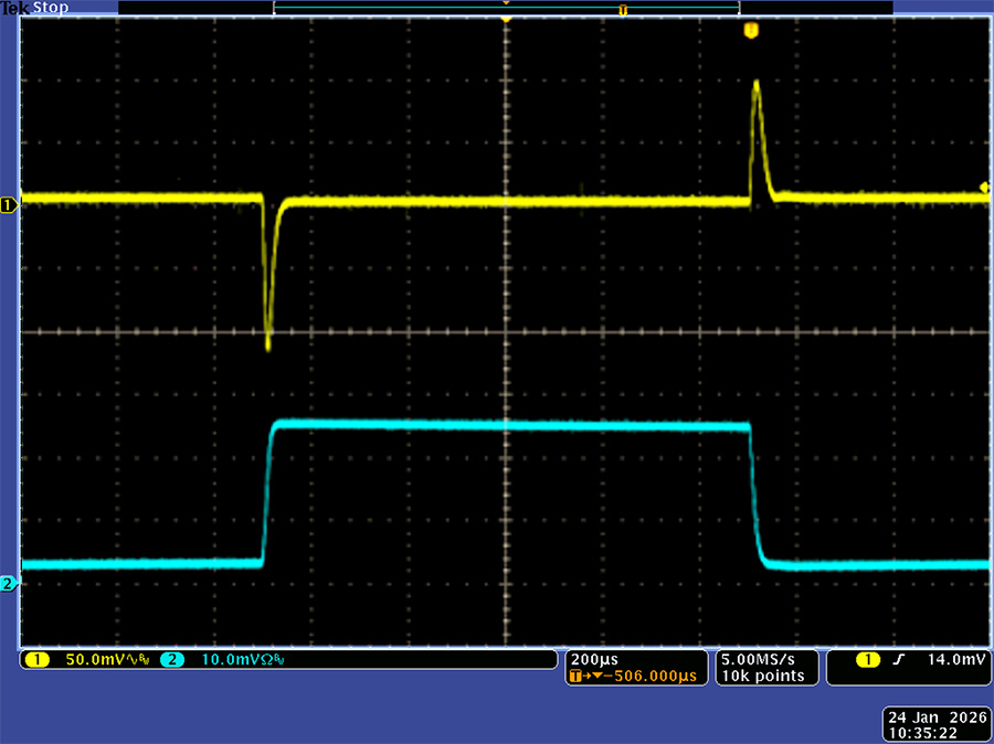
For the smaller-die HEMT variant, the transient load step was verified from 0.05 A to 0.5 A. Driven by a tighter internal parasitic capacitance profile, the voltage loop recovers within ~40 µs, restricting the maximum voltage deviation to a nominal 110 mV (Figure 7).
Figure 7: EPC7C024 Current Step-Change Response: 0.05A to 0.5A
Value Proposition & Broadband System-Level Implications
The demonstrated performance of eGaN HEMTs in continuous linear regulation alters high-reliability aerospace design trade-offs. Traditionally, spacecraft power distribution networks require separate semiconductor qualification pipelines for high-frequency payloads and continuous DC regulation. Proving that eGaN technology can operate as a stable, radiation-tolerant LDO pass element enables broad architectural consolidation beyond localized efficiency parameters.
Spectral Versatility: Unifying DC and RF Power Infrastructure
The core architectural benefit highlighted by Tony Marini revolves around the broadband utility of the GaN substrate. While Gallium Nitride has established a definitive role in high-frequency switching power converters and RF power amplifiers, its deployment in zero-frequency (DC) analog applications completes a crucial design continuum.
This spectral versatility yields significant advantages for spaceflight systems:
Component Qualification Consolidation: Utilizing a single, inherently radiation-hardened semiconductor technology across the DC-to-RF frequency spectrum reduces the overhead associated with establishing diverse component qualification lifecycles.
Elimination of Radiation Shielding Mass: The structural immunity to Total Ionizing Dose (TID) degradation simplifies structural design. Designers can omit heavy localized spot shielding around linear voltage regulators feeding sensitive payloads.
System Drift Redundancy Mitigation: Because the physical control nodes do not undergo the radiation-induced charge-trapping typical of silicon-oxide interfaces, the need for complex digital calibration or telemetry compensation networks to correct for rail drift over long mission lifespans is eliminated.
Minimization of Worst-Case Design Margins
Silicon linear regulators require over-designed loops to counter orbital parameter drift. Conversely, the eGaN control loop maintains stable, oscillation-free transient responses without complex compensation because its transconductance thresholds remain unchanged over the spacecraft’s operating life. This proves eGaN HEMTs act as reliable continuous DC regulation elements, giving aerospace designers a single, uniform semiconductor platform handling everything from direct current to microwave frequencies.
Implementation Guidelines
The verification of eGaN HEMTs within LDO linear regulator topologies provides a clear framework for high-reliability aerospace power distribution networks. By evaluating the structural boundaries, thermal dynamics, and loop behavior analyzed in the preceding sections, designers can implement unified guidelines to maximize system reliability in hostile orbital environments.
Component Implementation Guidelines
To replicate the deterministic, oscillation-free performance recorded on the evaluation hardware, space-grade system layout execution must adhere to three strict design constraints:
Gate Drive Impedance and Stray Inductance Control: Due to the high transconductance (gm) of eGaN devices, any parasitic inductance at the gate terminal can couple with the internal capacitances to induce high-frequency ringing. Gate routing traces must be minimized to short, wide geometries and placed on the same PCB layer as the analog error amplifier whenever possible.
Dynamic Thermal Layout Decoupling: Linear pass elements operating under constant input-to-output voltage differentials face continuous thermal dissipation (PD = ΔV . Iout). Designers must maximize the use of planar ceramic helper pads (such as aluminum nitride structures) to route heat laterally into internal board copper planes, preventing localized hot spots from shifting the operating thresholds of surrounding low-voltage reference circuits.
External Sense Resistor Placement: To preserve the native, uncompensated dropout voltage performance of the GaN substrate, the current sense resistor must remain physically outside the closed voltage feedback loop. However, designers must account for its continuous series ohmic loss when calculating the total worst-case dropout ceiling at the system level.
Conclusions
Integrating eGaN HEMTs into linear regulation architectures successfully bridges a critical gap in spacecraft power infrastructure. This architecture demonstrates that Gallium Nitride is no longer restricted to high-frequency switching converters or RF payloads; it can operate as a reliable, stable pass element for continuous DC regulation.
Ultimately, this structural validation allows aerospace engineers to implement a single, unified semiconductor platform across the entire DC-to-RF frequency spectrum. Consolidating the component procurement lifecycle, eliminating local radiation shielding mass, and removing end-of-life parameter drift margins allow for the development of lighter, more efficient, and highly ruggedized power electronics optimized for deep-space and long-duration orbital missions.
The recent investigation into a half-Möbius ring-shaped molecular system has attracted interest not only because of the molecule’s atypical topology, but because it represents a milestone in computational science. The system belongs to a growing class of molecular structures whose electronic behavior is so intricate that conventional simulation becomes increasingly difficult to scale even on the fastest digital computers.
In a study published in the journal Science, researchers describe the creation of the first molecule exhibiting a form of quantum matter that had not even been predicted before.
The molecule (C13Cl2) was assembled atom by atom, thanks to a team of scientists from IBM, Oxford, the University of Manchester, ETH Zurich, École Polytechnique Fédérale de Lausanne, and the University of Regensburg. The team used quantum-centric supercomputing, a new paradigm that, operating quantum and classical systems in tandem, is accelerating the transformative role of quantum computing (QC).
Domains where QC will excel
Among the many proposed applications of QC—from cryptography to a large class of optimization problems—molecular simulation remains one of the most scientifically solid and potentially consequential. The reason is fundamental: molecules are quantum systems themselves. Their behavior is governed by the laws of quantum mechanics at every level, from bond formation to chemical reactivity and electronic transport mechanisms. Put more directly, chemistry is quantum computation per se—performed by nature.
The promise of QC lies in reproducing this computation artificially, allowing scientists to model molecular systems with a level of fidelity and accuracy that may eventually exceed what classical computing can efficiently achieve.
This matters not only for analyzing molecules that already exist in nature. More importantly, it makes it possible to simulate entirely new molecular systems before they are synthesized—materials, catalysts, battery chemistries and functional compounds that have never existed anywhere in our world.
Molecules as an ensemble of atoms
At a macroscopic level, molecules appear simple arrangements: atoms connected through chemical bonds, forming stable structures governed by well-established rules. But the analysis of molecular behavior becomes far more complicated when viewed at the electronic-structure level.
A molecule is fundamentally a many-body quantum system composed of strongly-interacting nuclei and electrons. The nuclei define the molecular framework, while electrons determine most of the molecule’s physico-chemical behavior: bonding, stability, reactivity, optical response, conductivity, and magnetic properties.
The complexity stems from the fact that each electron interacts simultaneously not only with the electric fields generated by the nuclei, but also with other fields associated with every other electron and, additionally, external disturbances, including thermal fluctuations. All these interactions create a strong coupling among all system elements whose full quantum state description becomes computationally expensive.
Mathematical formalism of quantum systems
The mathematical framework of quantum mechanics is built on state vectors defined in an abstract Hilbert space—which may even be infinite-dimensional—and on linear operators, representing physical observables such as position, momentum, and energy, acting on the system’s state. As a useful conceptual analogy, albeit imperfect, quantum states can be viewed as a generalization of vectors in three-dimensional Euclidean space.
For molecular systems, the central mathematical object is the Hamiltonian, the operator describing the total energy of the system—both kinetic and potential—from nuclei and electrons, as well as interactions with external fields or perturbations. Treating molecular quantum mechanics boils down to solving the Schrödinger equation associated with this Hamiltonian to determine the molecular wavefunction, which describes the system’s quantum state.
From the wavefunction, we can determine total energy, electronic density, transition probabilities, reaction pathways as well as molecular dynamics under perturbations. In quantum mechanics, electrons do not move in classical trajectories around the nuclei, as if they were deterministic orbits. Instead, they fill up orbitals, quantized wavefunctions that describe where the electron is likely to be found, and what energy states it is allowed to be in.
The resulting probability density is commonly depicted as a diffuse cloud surrounding the nucleus.
The extreme computational difficulty arises because the wavefunction exists in a Hilbert space whose dimensionality grows exponentially with the number of interacting particles. This exponential scaling constitutes one of the fundamental bottlenecks of computational chemistry, making exact simulations feasible solely for small molecular systems.
Classical computational methods
Classical computation can only address this problem through approximation methods that have enabled major advances in drug development, catalyst design, battery research, and materials engineering.
However, there are important classes of molecular systems where approximation becomes increasingly difficult. Examples include systems with strong electron correlation, highly entangled electronic states, nontrivial topology, and unusual quantum phase behavior.
Half-Möbius molecule
Typically, a ring of atoms connected in a molecule is said to be “topologically trivial” if, by tracing their atomic orbitals around the ring, one can return to the starting point after one single loop.
To visualize a half-Möbius molecular system, let’s consider a Möbius strip first. This is a surface with only one side and one continuous edge, created by twisting a strip or ribbon by 180º degrees and then joining its ends.
In a half-Möbius molecular system, a topological twist by 90º is introduced into a ring-shaped orbital structure. This means that for the electron cloud to complete a full twist, four successive loops are necessary. This half-Möbius topology defines an entirely new class of molecules, distinct from known molecular topologies. Additionally, the system can revert between a right-handed half-Möbius, a left-handed half-Möbius, and the topologically trivial configuration.
The effect of this twist is to modify the symmetry and energy spectrum, causing the electronic energy levels and electron distributions to change unpredictably. As a result, electrons experience constraints that diverge from those in conventional cyclic molecules, such as hexagonally symmetric benzene (C6H6).
The exotic orbital re-configurations are caused by subtle interactions among topology, geometry, and electron correlation, making the system particularly challenging to model with standard computational techniques.
Quantum computing for chemistry
Simulating quantum systems with classical computers becomes inefficient because classical digital hardware cannot represent quantum states directly.
Quantum computers leverage qubits—rather than bits—which can be prepared in superpositions of states.
It is also possible to entangle multiple qubits, which is turn enables the processor to replicate quantum correlations.
The usefulness of quantum computers therefore, lies in their ability to efficiently represent certain classes of quantum states, including those relevant to molecular systems.
A quantum processor can be constructed that encodes molecular wavefunctions into qubit states that evolve according to the rules of quantum mechanics. This enables direct insight into molecular properties such as ground-state energies, excited states, and chemical reaction pathways.
In reality, current quantum hardware faces significant constraints such as noisy gates, short coherence times, limited qubit counts, and immature error correction schemes. For this reason, near-term quantum chemistry relies heavily on a combination of quantum and classical approaches.
One such paradigm is the Variational Quantum Eigensolver (VQE). In this hybrid framework, a quantum processor prepares candidate molecular states, while a classical optimizer iteratively adjusts parameters to minimize the energy expectation value and approximate the ground state, from which relevant chemical properties can be inferred.
Albeit limited in scale, such methods have already proved meaningful progress in molecular simulation.
How to predict new molecules
The truly transformative application of quantum simulation may be the exploration of brand-new chemical compounds, potentially in huge numbers.
Quantum simulation could allow researchers to computationally search this vast design space, identifying stable and useful molecular systems before they are even synthesized.
This could fundamentally change the workflow for finding new molecules. Instead of an iterative experimentation process, scientists may propose some new molecular alternatives, simulate and optimize their quantum behavior, and, finally, synthesize only the most promising candidates.
This approach can enable numerous important applications, among them the design of matter with entirely novel properties.
Far from being a mere scientific curiosity, the half-Möbius system represents a far-reaching advance in molecular science, enabling the design and control of quantum systems rather than simply their observation.
What to expect
Chemistry is increasingly becoming the science of designing matter and QC could become one of the most important tools enabling this transition.
The long-term goal is not merely faster simulation. It is the ability to encompass molecular systems that classical computation cannot efficiently access, including structures and materials that have never existed in nature.
If that promise materializes, quantum computers will become engines for discovering entirely new forms of matter, bringing to life the vision first articulated by Richard Feynman.
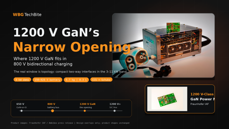
Most concept cars never reach a showroom. They exist to prove a direction the maker is willing to fund. The 3 kW bidirectional charger Fraunhofer IAF showed at PCIM Europe 2026 reads the same way.
The power number is almost a distraction. At 3 kW, this off-board, single-phase, 800 V DC charger is slower than the 11 kW and 22 kW on-board chargers already in cars. What makes it worth a second look is the device inside it: a 1200 V-class GaN module aimed at a part of the 800 V battery market that neither today’s GaN nor today’s SiC fits cleanly.
So the question this demo really poses is narrow and concrete: where does 1200 V GaN actually belong?
The awkward middle of 800 V charging
GaN4EmoBiL, the project behind the demo, started in 2023 with a problem most spec sheets hide. For an 800 V battery doing two-way charging, every device choice is a compromise:
• SiC works and is qualified, but it carries a cost premium.
• Silicon is cheap, but efficiency and power density run out early.
• 650 V GaN-on-Si is efficient and affordable, yet too low in voltage for an 800 V bus without cascoding or extra stages that eat the savings.
That leaves an opening between 650 V GaN and 1200 V SiC. The project’s stated goal is to fill it with a low-cost 1200 V device that covers an 800 V bus without those workarounds.
Getting GaN to hold 1200 volts
The harder part is physics. Lateral GaN-on-Si has been in production for years, but the conductive silicon underneath creates a vertical breakdown path that keeps most commercial parts at 650 V.
In 2024 Fraunhofer IAF laid out three routes past that ceiling:
1. GaN-on-Si HEMTs, pushed through material and device optimization to over 1200 V static blocking, with switching demonstrated above 1100 V.
2. GaN-on-insulator HEMTs, the centerpiece – replacing conductive silicon with sapphire, SiC, or GaN carriers to weaken the vertical breakdown path and lift the voltage further.
3. Vertical GaN, a longer-term bet the institute frames on a roughly ten-year horizon.
The insulating-substrate route matters most here, because 650 V parts leave too little voltage margin for an 800 V battery, while 1200 V starts to clear it.
Bidirectional is the harder half
Voltage is only one wall. A two-way charger has to pull energy from the grid and push it back to a home, a battery, or the grid, which means blocking and conducting in both directions, plus the control and protection that come with it.
This is where the monolithic bidirectional switch Fraunhofer IAF disclosed in 2025 fits. Built in GaN-on-insulator with integrated free-wheeling diodes, it blocks and conducts both ways in one device instead of two back-to-back transistors, which can cut chip area and conduction loss.
The contrast with the market is sharp. Commercial bidirectional GaN today still clusters at 650 V. Infineon’s CoolGaN BDS is the clearest example, aimed at solar microinverters and server power. Fraunhofer IAF is reaching straight for 1200 V and an 800 V battery. That is the most distinctive thing about the route, and also the reason it is still in the lab rather than on a shelf.
Why 3 kW, and why now
Seen as a charger, 3 kW looks underpowered. Seen as an interface, it looks deliberate. The demonstrator weighs 5.7 kg, fits in 8.3 liters, spans a 150-920 V battery range, and carries CCS plus Schuko connectors. It is built to sit in a garage or move with you, not to fast-charge.
The timing tracks the market it serves. University of Stuttgart’s part of the project targets a near-product 3.4 kW off-board cable now and an 11 kW three-phase on-board concept later, on a low-cost 1200 V GaN route using sapphire or QST substrates, with V2H and V2G reliability evaluated past 60,000 hours.
And the demand side is arriving. Volkswagen and Elli plan a vehicle-to-grid service for private customers in Germany from Q4 2026, with pre-registration opening in mid-2026. A compact, affordable two-way DC interface has a place in that world that a 22 kW charger does not.
What this does to the SiC line
Putting 1200 V GaN into an 800 V two-way charger invites the obvious framing: GaN coming for SiC. That read is premature.
In fast charging, traction inverters, and storage PCS, SiC keeps a mature module base, automotive qualification history, and customer trust. GaN’s path into those sockets runs through full system validation, well beyond datasheet parameters.
Where the line could actually move is narrower:
• Bidirectional topologies, where one 1200 V monolithic switch can replace two reverse-series SiC devices and save area, loss, and gate-drive complexity.
• System cost, where a single 1200 V GaN stage avoids the cascoding an 800 V bus forces onto 650 V parts.
• The 3-11 kW band, where compact, light, two-way DC interfaces reward GaN’s frequency and density.
The competition is drifting away from raw material comparisons toward a sharper question: in which power and topology window is the system simpler and cheaper?
The line the public record hasn’t drawn
Here is what keeps this from being a finished story. The demo runs a 1200 V GaN module. Fraunhofer IAF has separately built a 1200 V monolithic bidirectional switch. The intuitive move is to assume the second is inside the first.
The public materials do not confirm that. “1200 V” describes the device voltage class of the module; “bidirectional” describes what the system does. Whether the 2025 MBDS actually sits in this 3 kW box is a connection the disclosures stop short of making.
Everything else is still missing too: efficiency curves, thermal data, dynamic Ron, gate reliability, the full 60,000-hour result, BOM comparisons against SiC, a path to volume. The technical direction is legible. Whether 1200 V GaN can carry real energy through an 800 V interface, and whether the switch already exists to do it, is the part the next data release has to answer.
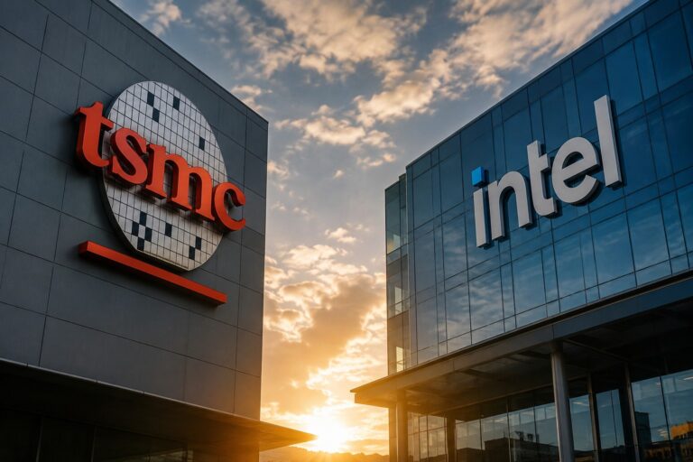
Over the past few weeks, a series of seemingly unrelated headlines has emerged across the semiconductor industry. MediaTek announced support for both Intel’s EMIB and TSMC’s CoWoS, giving customers greater flexibility in choosing advanced packaging platforms. Reports also suggest that SK hynix is evaluating Intel’s EMIB for future HBM integration, while TSMC continues to expand CoWoS capacity to support relentless AI demand. At first glance, these appear to be independent business decisions.
But are they? Could these developments actually be telling the same story?
Everyone is watching the AI chip race.
The conversation continues to revolve around larger models, faster GPUs, higher HBM bandwidth, and increasingly advanced process nodes. Those metrics have defined semiconductor leadership for decades, and they remain important. Yet, taken together, the latest industry moves suggest that another dimension is rapidly becoming just as critical. As AI systems become larger, more heterogeneous, and increasingly interconnected, the challenge is no longer limited to designing the fastest processor. Instead, the focus is gradually shifting toward something much broader: how do you manufacture these increasingly complex systems—reliably, economically, and at hyperscale?
Once that question becomes the priority, the recent headlines begin to make much more sense.
Intel is doubling down on EMIB. TSMC is expanding CoWoS capacity faster than ever. HBM suppliers are broadening their ecosystem partnerships. Hyperscalers are evaluating multiple advanced packaging strategies instead of depending on a single solution. Seen individually, each announcement reflects a specific business decision. Viewed collectively, however, they point toward the same structural transformation. The AI race is no longer just a competition between chips.
It is becoming a competition between manufacturing ecosystems.
Why EMIB and CoWoS Reflect Different AI Manufacturing Strategies
This is also why I think framing the discussion as Intel versus TSMC overlooks the broader context. EMIB and CoWoS are not simply competing packaging technologies. Rather, they represent two different philosophies for scaling AI infrastructure. CoWoS is built around maximizing integration through a large silicon interposer, pushing bandwidth and interconnect density to support the largest AI accelerators. EMIB takes a more modular approach, embedding silicon bridges only where ultra-high-density interconnects are required, balancing performance with manufacturing flexibility and silicon efficiency.
The objective is the same. The engineering philosophy is different. That distinction matters because each philosophy exists independently of the other. Instead, both exist because the AI industry is searching for the most effective way to scale increasingly complex heterogeneous systems.
That, in my view, is the real story.
EMIB and CoWoS are not the story themselves. They are the first visible signs that the AI industry is entering the manufacturing era. As a result, the same shift is driving investment in HBM, advanced substrates, heterogeneous integration, OSAT capabilities, thermal management, testing, and supply-chain resilience. These are no longer supporting technologies operating quietly in the background.
They are becoming strategic differentiators.
Taken together, these trends point to a much larger transformation. EMIB and CoWoS are only the opening chapter. The real race is no longer about building the fastest AI chip. It is about orchestrating the technologies, manufacturing capabilities, supply chains, and strategic partnerships required to scale AI infrastructure.
Because, in the end, AI is no longer a race to build the best chip. It’s a race to build the best ecosystem.
The rapid expansion of artificial intelligence is reshaping the semiconductor industry, with power management emerging as one of the most critical technologies enabling next-generation AI infrastructure. Against this backdrop, Infineon Technologies has been recognized by Gartner as the “Company to Beat” in AI data center power semiconductors, highlighting the company’s comprehensive strategy for addressing the growing energy demands of modern AI systems.
Unlike traditional semiconductor suppliers that focus on individual sections of the power chain, Infineon has developed a complete portfolio spanning the entire power delivery architecture. Its solutions cover every stage of energy conversion—from the electrical grid to the processor core—including solid-state transformers, power supply units, energy storage systems, intermediate bus converters, and processor-level voltage regulation. This end-to-end approach enables higher efficiency, improved reliability, and greater system optimization, all of which are becoming increasingly important as AI servers continue to increase in power density.
The explosive growth of generative AI and large-scale data centers has dramatically increased power consumption while placing greater emphasis on thermal management and energy efficiency. These challenges are accelerating the adoption of advanced power semiconductor technologies such as silicon carbide (SiC) and gallium nitride (GaN), areas where Infineon has invested heavily over the past several years.
According to Gartner, Infineon’s combination of broad product coverage, manufacturing capabilities, and early investment in next-generation power technologies positions the company ahead of many competitors. While competition in SiC and GaN devices continues to intensify, particularly from vendors targeting individual stages of the power architecture, Infineon’s system-level expertise provides a significant competitive advantage.
The company expects the AI market to become an increasingly important contributor to its business, projecting approximately €2.5 billion in AI-related revenue by fiscal year 2027. This forecast reflects not only rising demand for AI servers but also the need for highly efficient power conversion throughout hyperscale data centers as operators seek to reduce operating costs and improve sustainability.
As AI infrastructure continues to evolve, power electronics are becoming a strategic differentiator rather than simply a supporting technology. Efficient energy conversion, high-performance semiconductor devices, and optimized power architectures will play a central role in enabling the next generation of AI computing. Infineon’s recognition underscores how leadership in power semiconductors is becoming essential for meeting the industry’s growing performance and efficiency requirements while supporting the continued expansion of AI-driven data centers.
We’ve judged technological progress by faster processors, denser memory, more sophisticated software for decades. Energy was essential but typically treated as a background utility, important but rarely decisive in strategy.
That paradigm is shifting quickly.
The explosive growth of artificial intelligence, hyperscale data centers, advanced semiconductor manufacturing and electrification is putting unprecedented strain on global energy infrastructure. So the talk is moving away from computational performance to a bigger question: can the power ecosystem keep up with digital innovation?
In its latest report, GeoTechNexus examines this metamorphosis, stating that energy has evolved from a simple operational cost to a strategic asset. More importantly, it investigates why power electronics have become one of the crucial enabling technologies for the next-generation digital infrastructure.
The report takes a look beyond processors and AI accelerators to the technologies that work behind the scenes, such as power semiconductors, energy conversion systems and the infrastructure that makes for reliable, efficient and scalable electricity delivery. These technologies are playing an ever-increasing role in determining how fast new computing capacity can be brought online, and how efficient modern digital systems can be.
The report also points to another important dimension – the growing interaction between technology, industrial policy and geopolitics. Manufacturing capacity, critical materials, energy availability and supply-chain resilience are becoming central to the competitiveness of both companies and countries.
The report is more than a description of the current market trends. Instead, it provides a broader strategic context for understanding why energy is becoming one of the defining variables of the high-tech economy, and what that means for semiconductor companies, data-center operators, policymakers and investors.
As the pace of AI adoption quickens and electrification picks up across industries, the ability to efficiently capture, control and convert electrical power may prove to be as important as advances in computing itself.
Readers seeking a deeper analysis of these changing dynamics will find it in the full report, based on industry research and expert insights, and relevant to the future of electronics, semiconductors, power systems and global technology strategy.