


Vertical GaN-on-silicon is widely seen as a route to cost-effective power electronics and high-resolution micro-LEDs, combining GaN’s superior breakdown field and electron mobility with the large-diameter, low-cost wafer infrastructure already in place for silicon. The architecture has, however, been held back by a persistent materials problem: conventional epitaxial buffer layers introduce high vertical electrical resistance, blocking the current path required for vertical device operation. A new study published in Advanced Physics Research presents a practical solution.
The work, led by Fumio Kawamura and colleagues, introduces a universal sputtering-based strategy to grow high-quality GaN epitaxial films on Si(111) substrates with exceptionally low vertical resistance, ohmic electrical behavior, and robust thermal stability.
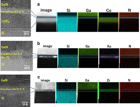
The core of the approach is a deliberately engineered nucleation layer. The technique centers on the in-situ formation of a sub-nanometer (0.5 nm) silicide-based template via rapid thermal annealing (RTA). By keeping this interlayer below one nanometer, the researchers preserve epitaxial registry with the underlying silicon while simultaneously creating a conducting interface that supports vertical current flow, the two requirements that prior buffer strategies struggled to satisfy simultaneously.
What makes the result particularly significant for manufacturability is its breadth. The method demonstrates unprecedented versatility across 25 different metallic species, meaning the silicide template is not restricted to a single metal system. Engineers can select from a wide range of metals based on process constraints, thermal budget compatibility, or integration requirements, without sacrificing low-resistance characteristics.
The sputtering deposition route is also noteworthy from a process integration standpoint. Sputtering is a mature, high-throughput technique already present in most compound semiconductor fabs, making adoption significantly more straightforward than approaches that require specialized MOCVD modifications or novel precursor chemistries.
From a device perspective, the immediate beneficiaries are vertical GaN power transistors and diodes, where current must flow perpendicular to the wafer surface, and even modest series resistance in the buffer degrades on-state performance and efficiency. High-resolution micro-LED arrays represent a second application space: vertical current injection through a conductive buffer enables uniform pixel-level control, which is essential for display applications targeting augmented and virtual reality hardware.
The broader context is a maturing push to scale up the adoption of GaN power and optoelectronic devices on silicon substrates. Native GaN substrates remain expensive and have limited diameters; 200 mm and 300 mm silicon wafers are orders of magnitude cheaper and available in high volumes. Closing the remaining epitaxial engineering gaps, of which vertical resistance has been one of the most stubborn, is a prerequisite for GaN-on-Si to compete on cost without compromising device specifications.
By combining a well-characterized deposition method, a sub-nanometer interlayer that avoids disrupting crystal quality, and demonstrated compatibility across a broad set of metallic systems, this work offers a transferable and scalable process for the vertical GaN device community.
