

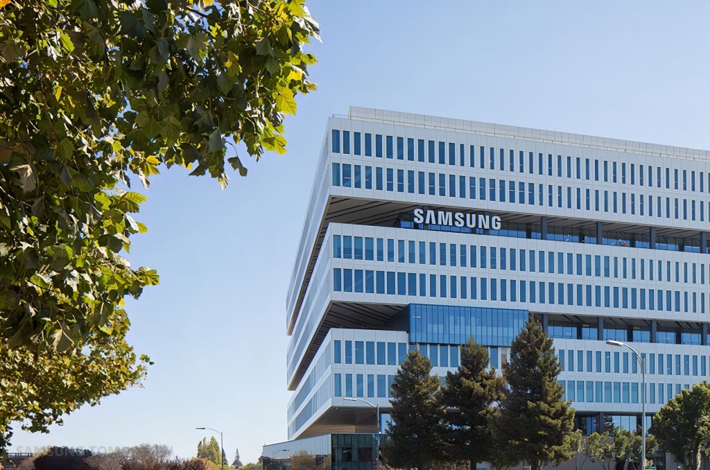
Samsung Electronics is reportedly shifting its gallium nitride (GaN) semiconductor strategy toward foundry services after encountering difficulties in expanding its GaN device business. According to reports from The Elec, the company is prioritizing outsourced manufacturing opportunities as customer demand for GaN foundry capacity continues to grow.
Industry sources cited in the report said that Samsung struggled to secure final purchase orders for its GaN power devices after customer evaluations reportedly identified performance and quality limitations. These issues are said to have delayed progress toward mass production. The report also noted that Samsung exited a government-backed GaN development project before completion.
One reported challenge involved on-resistance (RDS(on)), a key parameter affecting power efficiency and heat generation in power semiconductors. According to the report, Samsung’s GaN devices did not consistently meet customer requirements for low resistance and efficiency performance. Another issue reportedly involved the company’s inability to offer complete GaN power modules, which many customers prefer over standalone devices for easier system integration.
While the discrete device business has faced challenges, Samsung’s GaN foundry activities are reportedly progressing more successfully. The company is said to have secured multiple foundry customers and could begin operations as early as July. The report suggests that customers may be more willing to diversify GaN production across multiple foundries because GaN manufacturing generally requires lower photomask redesign costs than conventional silicon processes.
However, GaN manufacturing still presents technical challenges, particularly in maintaining stable electrical characteristics and resistance uniformity during wafer processing. Competition in the sector is also increasing, with domestic rivals including DB HiTek and SK keyfoundry also expanding their GaN foundry activities.
Samsung’s broader strategy in power semiconductors reportedly includes renewed investment in silicon carbide technologies to strengthen its position in next-generation wide-bandgap semiconductor markets.
