



In recent years, planetary exploration missions have achieved significant technological progress, with approximately five robotic rovers successfully deployed on Mars, the most recent being the Perseverance rover. Silicon carbide (SiC) devices are playing an increasingly important role in space exploration, enabling scientists to perform more detailed investigations of planetary surfaces and atmospheres while also supporting future preparation for human missions beyond Earth. Mars is an extremely cold environment, with an average surface temperature of around −70°C. Under such conditions, conventional silicon-on-insulator (SOI) integrated circuit technology can be employed in rover electronic systems. However, these silicon-based ICs typically have a maximum operating temperature near 300°C, beyond which their long-term reliability and performance cannot be maintained.
Venus is considered to be the sister planet of Earth because it has a similar size and composition, and surface exploration of this planet is expected to provide valuable information about Earth’s history. The average temperature on the surface of Venus is about 400°C, which is way above the maximum limit of the functioning of conventional Si-based electronic devices. Previous explorations sent to Venus have proved that these ICs only survived about 2 hours in that environment. This is where SiC devices prove to be powerful candidates. These wide band gap devices are suitable to be used for high-power and high-temperature applications.
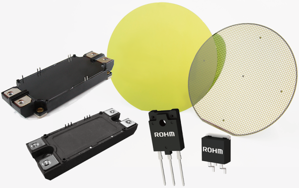
SiC-based devices for space exploration
The atmosphere of Venus is extremely dense and consists primarily of carbon dioxide (about 96.5%), while the planet’s surface temperature reaches approximately 450°C and the atmospheric pressure at the surface is around 92 atmospheres. Earlier Soviet Venus missions, including Venera 7 (1970), which operated for only 23 minutes, and Venera 13 (1982), also demonstrated very limited operational lifetimes because of the planet’s extremely harsh environmental conditions.
Space exploration landers are generally classified into three main categories: short-duration landers, long-duration landers, and mobile surface platforms. Short-duration landers typically operate for only a few hours and are mainly used to perform meteorological measurements and preliminary analysis of surface rocks and soil. Due to their limited mission time, silicon-based electronic devices combined with appropriate cooling strategies can still be used in these systems. In contrast, long-duration landers are designed to function for roughly 120 days and support extended monitoring of environmental parameters such as temperature, pressure, wind speed and direction, atmospheric composition, and seismic activity. Mobile surface platforms, meanwhile, are intended for mineralogical investigations and panoramic imaging of planetary terrain. For both long-duration landers and mobile exploration platforms, conventional silicon electronics are not suitable because silicon loses its semiconductor functionality above about 300°C. As a result, silicon carbide (SiC) technologies are being actively explored as a more reliable alternative for extended missions in extreme environments.
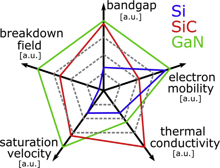
In addition to having a bandgap approximately three times wider than that of silicon (3.2 eV compared with 1.1 eV), silicon carbide is capable of maintaining its semiconductor properties at temperatures approaching 600°C, whereas silicon devices cannot operate reliably beyond roughly 300°C. Owing to this wider bandgap, SiC devices can tolerate higher voltages, greater power densities, stronger radiation exposure, and lower off-state leakage currents compared with conventional silicon components. Furthermore, SiC exhibits excellent thermal conductivity, enabling faster heat dissipation than many other semiconductor materials. This allows SiC power devices to operate at elevated power levels while effectively managing the excess heat generated during operation. In addition, SiC technology offers strong high-voltage blocking capability, reduced on-resistance, and reliable performance at elevated temperatures, supported by a breakdown electric field roughly ten times higher and a thermal conductivity about three times greater than that of silicon.
Challenges in SiC-based devices for space exploration
Although silicon carbide (SiC) technology has made significant progress in recent years, it is still less mature than conventional silicon-based manufacturing platforms. Compared with silicon, SiC technology currently faces limitations in wafer diameter availability, fabrication cost, and transistor scaling capability. The channel length of present-day SiC transistors typically remains in the micrometer range, similar to the dimensions achieved by silicon technologies in the 1980s. As a consequence, SiC-based electronics generally operate at lower switching speeds than advanced silicon devices, which restricts their use in highly complex circuits requiring high-frequency performance.
One of the main challenges in SiC fabrication is related to the intrinsic properties of the material itself. Because SiC is extremely hard—approaching diamond-like mechanical characteristics—its crystal growth and processing require higher temperatures, longer processing times, and greater energy consumption than silicon. In addition, the material’s high optical transparency and relatively large refractive index, particularly for the widely used 4H-SiC polytype, make inspection for surface defects more difficult. These limitations can directly influence epitaxial growth quality and ultimately impact device yield.
Typical defects observed during SiC substrate manufacturing include crystalline stacking faults, surface contamination particles, micropipes, pits, scratches, and staining. Studies have indicated that such defects tend to occur more frequently in 150 mm wafers compared with 100 mm substrates, potentially affecting the reliability and performance of SiC-based electronics intended for demanding environments such as space exploration. Furthermore, SiC processing presents additional challenges related to longer production cycle times, higher fabrication costs, and difficulties in wafer dicing, since the material is both extremely hard and relatively brittle. Another limitation arises from the very low diffusion coefficients of dopants in SiC, which makes conventional diffusion-based impurity doping techniques largely impractical.
To address these material and processing constraints, several advanced fabrication approaches have been introduced in recent years. Material-level improvements include both bulk crystal growth and epitaxial layer development, where lightly doped layers with thicknesses typically ranging from about 5 to 100 µm are grown homoepitaxially using chemical vapor deposition (CVD) on off-axis SiC substrates. In parallel, process-level innovations such as ion implantation and in-situ doping during epitaxial growth are now widely adopted as key techniques for the fabrication of SiC power devices.
Conclusion
Beyond planetary missions such as those targeting Venus, many other high-power and high-temperature environments require the development of electronic systems capable of operating reliably under extreme conditions, where silicon carbide (SiC) technology offers clear advantages. Representative application areas include naval propulsion systems, aircraft engine electronics, hybrid and electric vehicles together with their charging infrastructure, railway traction platforms, high-voltage direct current (HVDC) transmission, flexible AC transmission systems (FACTS), photovoltaic energy generation, wind power installations, and smart grid architectures.
To further improve system efficiency while reducing the size and weight of electronic assemblies, SiC is increasingly recognized as a key enabling technology for next-generation power electronics. Recent technological progress indicates that SiC-based solutions are expected to progressively replace conventional silicon devices in many high-power and high-temperature applications over the coming years, supporting more compact, robust, and energy-efficient system designs.
References
[1] H. Kim, J. Bagherzadeh and R. G. Dreslinski, “SiC Processors for Extreme High- Temperature Venus Surface Exploration,” 2022 Design, Automation & Test in Europe Conference & Exhibition (DATE), 2022, pp. 406-411, doi: 10.23919/DATE54114.2022.9774769.
[2] T. Kimoto, “SiC technologies for future energy electronics,” 2010 Symposium on VLSI Technology, 2010, pp. 9-14, doi: 10.1109/VLSIT.2010.5556137.
[3] Friedrichs, Peter. (2007). Technological challenges for manufacturing power devices in SiC. 2007 International Conference on Compound Semiconductor Manufacturing Technology, CS MANTECH 2007.
