

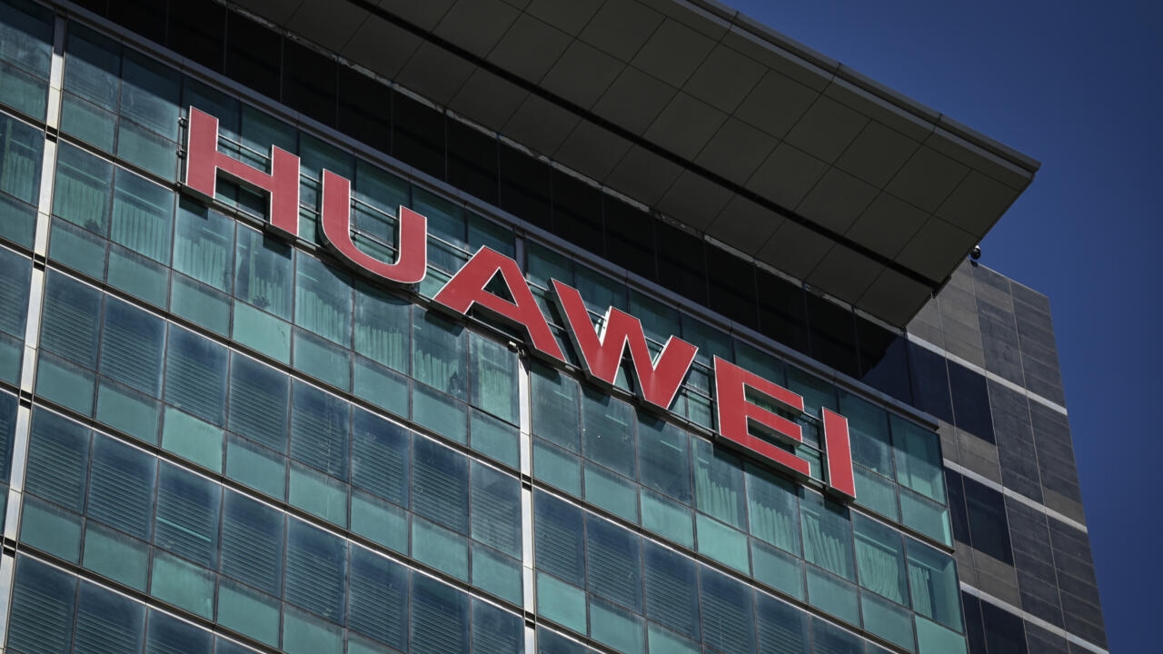
Huawei Technologies has outlined a new semiconductor design and manufacturing approach that the company claims could reduce its dependence on advanced lithography equipment subject to US export controls. The announcement was made during the International Symposium on Circuits and Systems (ISCAS) in Shanghai by He Tingbo, head of Huawei’s semiconductor division.
Since 2019, Huawei has faced a series of US-led sanctions that have limited the company’s access to advanced semiconductor technologies, including extreme ultraviolet (EUV) lithography systems used for manufacturing leading-edge chips below the 5 nm process node. These restrictions have significantly affected China’s ability to produce the most advanced AI and high-performance computing processors domestically.
During the presentation, Huawei stated that it expects to produce next-generation 1.4 nm chips by 2031, positioning its roadmap close to that of leading foundries such as TSMC, which has projected similar capabilities by 2028.
Huawei’s proposed approach departs from traditional semiconductor scaling models based on Moore’s Law, the long-established principle stating that transistor density on integrated circuits doubles approximately every two years. Instead of focusing primarily on reducing transistor dimensions, Huawei introduced what it calls the “Tau Scaling Law,” also referred to as “Her’s Law.” The concept shifts optimization priorities toward reducing communication latency between functional blocks inside a processor rather than exclusively maximizing transistor density.
According to the company, this architectural approach addresses some of the physical limitations associated with continued transistor miniaturization, including power density, signal integrity and manufacturing complexity. Huawei stated that the new methodology enables competitive performance while potentially reducing reliance on EUV-based process scaling.
The company also revealed that the next generation of its Kirin processors, expected to launch later this year, will be the first products to adopt a new “LogicFolding” architecture based on the Tau Scaling concept. Huawei claims the design improves internal data communication efficiency and supports future AI-oriented workloads.
Industry analysts view the announcement as a signal that Huawei is pursuing alternative semiconductor development paths to mitigate the impact of export restrictions and strengthen China’s domestic semiconductor ecosystem. The company’s long-term roadmap is also expected to intensify competition and geopolitical tensions surrounding advanced AI and semiconductor technologies.
