


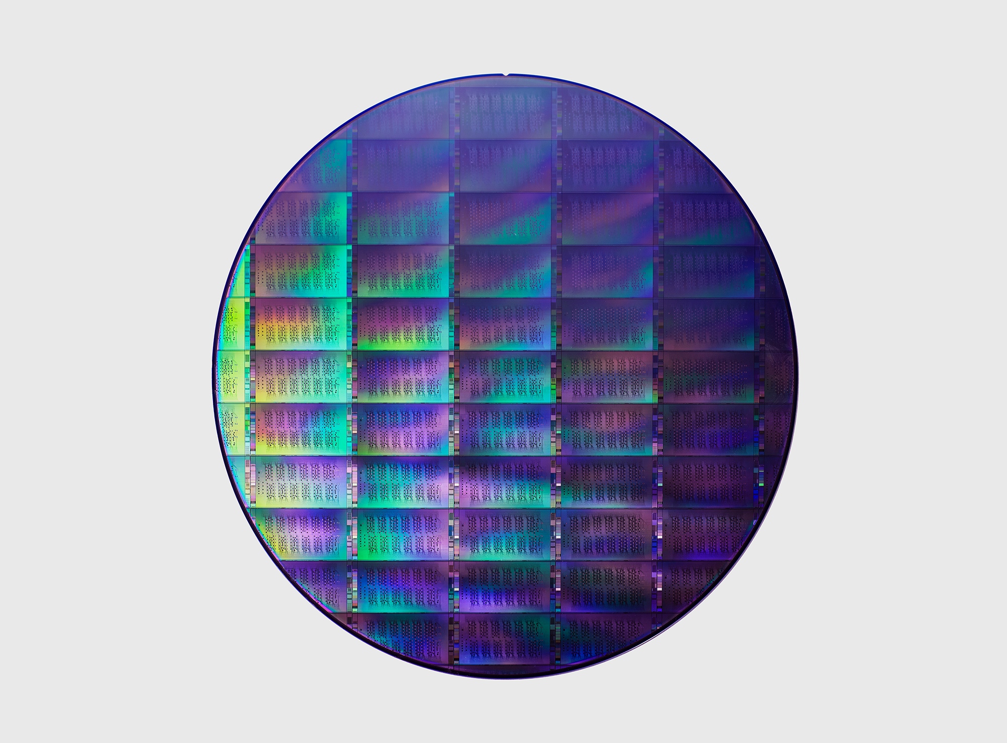
IBM and the U.S. Department of Commerce have announced a Letter of Intent (LOI) to establish the first purpose-built quantum chip foundry in the United States, marking a major step toward strengthening the country’s leadership in quantum technology and semiconductor manufacturing. The initiative, backed by a proposed $1 billion award under the CHIPS Act, is intended to accelerate domestic quantum research, development, and wafer production for a broad ecosystem of quantum hardware companies.
The CHIPS funding would support the creation of Anderon, a new standalone company formed by IBM to operate as a dedicated quantum wafer foundry. Alongside the proposed federal support, IBM plans to invest an additional $1 billion in cash and contribute intellectual property, manufacturing assets, and experienced personnel. Additional investors are expected to participate as the company expands.
Headquartered in Albany, New York, Anderon is expected to become America’s first pure-play quantum foundry, operating advanced 300-millimeter wafer manufacturing lines tailored specifically for quantum technologies. The project represents one of the largest U.S. government-backed quantum R&D efforts to date and is designed to help position the United States as a global leader in scalable quantum wafer manufacturing.
IBM emphasized that its broader quantum computing roadmap remains unchanged. The company stated that the new foundry initiative builds upon decades of expertise in both quantum computing and semiconductor fabrication. IBM has already demonstrated scalable quantum wafer technologies internally, creating a foundation for future commercialization and high-volume production.
As a dedicated foundry provider, Anderon plans to manufacture wafers for a variety of quantum technology developers worldwide. Initially, the company will focus on superconducting qubit wafers and associated supporting electronics, while future expansion plans include support for additional quantum computing modalities.
The foundry is also intended to strengthen the domestic supply chain for quantum hardware by providing a secure U.S.-based source for advanced quantum wafers. IBM aims to leverage its process expertise, manufacturing infrastructure, and specialized workforce to help establish reliable quantum production capabilities within the country.
According to the announcement, Anderon’s future manufacturing platform will support advanced 300mm quantum wafer technologies, including superconducting interconnects, through-silicon vias, and bump technologies. The facility is also expected to include sophisticated process design kits, inline testing and characterization capabilities, and baseline manufacturing flows that support rapid development cycles and scalable production.
Quantum computing is widely viewed as a transformative paradigm capable of solving highly complex scientific and industrial problems that classical supercomputers cannot solve. Potential applications span materials discovery, chemistry, optimization, cybersecurity, and advanced simulations.
IBM highlighted its longstanding leadership in the quantum sector, noting that it has deployed more than 90 quantum systems globally and maintains a network of over 325 Fortune 500 companies, research institutions, startups, and government agencies using its quantum computing infrastructure. The company has also collaborated extensively with organizations such as the National Institute of Standards and Technology, the Defense Advanced Research Projects Agency, and the United States Department of Energy to advance secure quantum manufacturing and large-scale fault-tolerant quantum computing.
IBM reiterated its goal of delivering the world’s first commercially useful large-scale fault-tolerant quantum computer by 2029. The launch of Anderon remains subject to final agreements and regulatory processes between IBM and the Department of Commerce following the newly announced Letter of Intent.
