Researchers at Rice University and TU Wien have achieved a major breakthrough in the study of quantum materials, experimentally measuring quantum entanglement in a quantum critical metal, a class of materials more commonly known as “strange metals.” Published in Nature Physics, the work is the strongest evidence yet that entanglement is a fundamental ingredient in the behavior of these exotic materials, and may open the door to advances in superconductivity and quantum computing.
Strange metals have puzzled physicists for decades, as they don’t follow the normal rules of electrical conduction. For ordinary metals like copper and gold, Fermi liquid theory works well. Strange metals work in a completely different way.
What are exactly Strange Metals? But, unlike normal metals like copper or gold, the electrical resistance of strange metals is directly proportional to temperature. They break the rules of the standard Fermi liquid theory, which considers electrons to be mostly independent particles. Instead, they are in a special state of matter where the electrons lose their individuality and act collectively, as a highly coordinated quantum system.
The new study concerns quantum entanglement, one of the most fascinating and counterintuitive ideas in modern physics.
What is Quantum Entanglement? It is a phenomenon where two or more particles become so entangled that the state of one instantaneously influences the other(s), no matter how far apart they are. This was called “spooky action at a distance” by Albert Einstein, who could not quite reconcile this with the classical ideas of space and time. In strange metals, though, entanglement goes far beyond pairs of particles, with billions of electrons acting collectively as a single quantum object.
The research team, headed by theoretical physicist Qimiao Si, wanted to test a long-standing prediction that entanglement is a defining feature of strange metals. Such a phenomenon has long been considered nearly impossible to measure in a complex many-electron system.
How did scientists measure such “spooky” things? They employed a sophisticated statistical device from quantum information theory known as Quantum Fisher Information, or QFI. They mathematically determined the degree of quantum entanglement present in a crystal by analyzing how the crystal responded to neutron scattering experiments. Their measurements showed that entanglement reaches a dramatic maximum at the quantum critical point—the exact point at which the material transitions from one quantum state to another. But the discovery does more than confirm theoretical predictions. It also deepens an unlikely link between condensed-matter physics and some of the most extreme objects in the universe.
Why do physicists talk about black holes? Strange metals and black holes seem to share a strange property – they dissipate energy at the maximum possible rate allowed by the laws of physics, a limit known as Planckian dissipation. Theoretical frameworks such as the Sachdev-Ye-Kitaev (SYK) model suggest that the intricate entanglement structure observed in strange metals could be mathematically similar to the physics at a blackhole’s event horizon, hinting at an interesting connection between quantum materials and gravity. The work has not only scientific significance, but could have profound technological ramifications.
What does this mean for us going forward? High-temperature superconductivity is often found together with strange metals. Deciphering the essence of this “entangled quantum soup” could aid scientists in creating materials capable of conducting electricity with no resistance at far higher temperatures — possibly even at room temperature. The breakthrough would revolutionize energy transmission, computing infrastructure, transportation systems and next-generation quantum technology development.
Their work opens a new experimental window on one of the most enduring mysteries of condensed matter physics, by making the first direct measurement of entanglement in a strange metal. Their findings not only confirm decades of theoretical work, but also bring scientists a step closer to tapping the extraordinary potential hidden inside quantum matter.
Everyone is talking about AI. Everyone is talking about GPUs. But I believe the next major bottleneck won’t be the processors themselves. It will be the infrastructure that connects them. As AI clusters continue to scale from thousands to tens of thousands of GPUs, moving data efficiently has become just as important as generating compute. This is why Co-Packaged Optics (CPO) has rapidly moved from a research topic to one of the semiconductor industry’s most strategic technologies.
However, the real question is no longer whether CPO works. The real question is whether the industry can manufacture it economically at hyperscale. History has shown that many promising semiconductor technologies do not succeed or fail because of performance alone. They succeed—or fail—because of manufacturing yield, supply-chain maturity, packaging capability, reliability, and field serviceability. In my opinion, CPO is entering exactly this phase.
The Supply Chain Is Becoming the Competitive Advantage
Much of the recent attention has focused on companies such as NVIDIA and Broadcom, but they represent only one part of a much larger ecosystem. The value chain behind CPO spans multiple highly specialized technologies:
Value Chain
Key Players
AI Accelerators & Switch ASICs
NVIDIA, Broadcom, Marvell
Silicon Photonics
Intel, Ayar Labs, Lightmatter, Celestial AI
Lasers & Optical Components
Coherent, Lumentum
Advanced Packaging
TSMC, ASE, Amkor
Fiber & Connectivity
Corning, Furukawa Electric
System Integration
Foxconn, Quanta, Wistron
End Customers
Microsoft, Google, Meta, Amazon
No single company can deliver CPO alone. Success depends on the maturity and coordination of the entire ecosystem.
Where I See the Biggest Challenges
From my perspective, the greatest risks are not optical bandwidth or photonic performance. They are manufacturing and operational challenges.
Advanced packaging remains one of the industry’s most constrained resources. CPO requires heterogeneous integration of switch ASICs, silicon photonics, lasers, and fiber interfaces with micron-level precision.
Thermal management is another critical hurdle. High-performance AI switch ASICs can consume well over one kilowatt of power, while optical components require stable operating temperatures to maintain performance and reliability.
Manufacturing yield becomes increasingly important because a defect in a single optical engine can affect an entire high-value assembly.
Finally, serviceability cannot be overlooked. Traditional pluggable optics allow failed modules to be replaced individually. With CPO, operators must rethink maintenance strategies when optical components become integrated with the switching platform.
These are engineering challenges—but they are also supply-chain challenges.
Looking Beyond the Headlines
AI chips and GPU demand dominate today’s headlines. Tomorrow’s competitive advantage may belong to the companies enabling the infrastructure behind them. The winners may not only be GPU designers. They may also include companies solving advanced packaging, silicon photonics, laser integration, optical testing, and large-scale manufacturing. CPO has already demonstrated what is technically possible. Now comes the harder challenge: industrialization.
Which companies will transform technical innovation into scalable manufacturing, resilient supply chains, and sustainable business models?
As AI infrastructure enters its next phase, I believe this question may matter more than who designs the next generation of chips.
A recent article in EE Times on Qilimanjaro Quantum Tech is a readable introduction to analog quantum computing but leaves some important technical and editorial opportunities for further exploration. The piece captures the excitement around analog quantum architectures well, however, a more neutral perspective would have been beneficial for comparison and assessment purposes.
The article clearly presents Qilimanjaro’s central argument: analog quantum systems may reduce the accumulation of errors by avoiding long sequences of gate operations. That said, a little more depth on the tradeoffs might be useful for readers to better appreciate the technical landscape. Analog systems are not necessarily ‘error free’; rather, they introduce different categories of challenges, including calibration precision, decoherence, control complexity, and scalability. In this sense, the discussion could benefit from viewing analog quantum computing as an alternative engineering approach to the problem rather than a reduction of it.
The most compelling part of the article is perhaps the discussion of AI as a future application area. This section could perhaps benefit from additional context. Quantum reservoir computing and exponentially growing neural network complexity are interesting, but still areas of active research, with industrial applicability still being explored.
A more technical perspective could add further depth to an already interesting story. An interesting question to the readers would be:
What evidence do we have today, beyond theoretical reservoir-computing papers, for analog quantum systems to meaningfully speed up AI workloads vs. increasingly specialized classical hardware?
This question appears especially pertinent considering the rapid evolution of ongoing classical AI infrastructure. GPUs, AI accelerators, and domain-specific architectures are making impressive strides in performance and efficiency. As such, evaluating future quantum-AI approaches will likely need to be judiciously benchmarked against an already fast-moving compute ecosystem.
Qilimanjaro remains a fascinating company pursuing a differentiated path in quantum computing, and its integration with hybrid HPC infrastructures is certainly worth watching. As quantum technologies mature, technical journalism can add particular value by complementing ambitious claims with broader technical context, benchmarking, and independent perspectives. A more quantitative context and a performance-oriented discussion would have provided the readers with a more complete picture of the opportunities and the limitations of analog quantum computing.
In conclusion, for optimization and quantum simulation, analog quantum computing may offer significant advantages for certain specialized applications. However, for building a general-purpose, universal quantum computer capable of running arbitrary algorithms of great length and complexity, most computer scientists still view fault-tolerant digital quantum computing as the more convincing long-term path.
Vertical GaN-on-silicon is widely seen as a route to cost-effective power electronics and high-resolution micro-LEDs, combining GaN’s superior breakdown field and electron mobility with the large-diameter, low-cost wafer infrastructure already in place for silicon. The architecture has, however, been held back by a persistent materials problem: conventional epitaxial buffer layers introduce high vertical electrical resistance, blocking the current path required for vertical device operation. A new study published in Advanced Physics Research presents a practical solution.
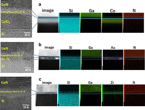
The work, led by Fumio Kawamura and colleagues, introduces a universal sputtering-based strategy to grow high-quality GaN epitaxial films on Si(111) substrates with exceptionally low vertical resistance, ohmic electrical behavior, and robust thermal stability.
The core of the approach is a deliberately engineered nucleation layer. The technique centers on the in-situ formation of a sub-nanometer (0.5 nm) silicide-based template via rapid thermal annealing (RTA). By keeping this interlayer below one nanometer, the researchers preserve epitaxial registry with the underlying silicon while simultaneously creating a conducting interface that supports vertical current flow, the two requirements that prior buffer strategies struggled to satisfy simultaneously.
What makes the result particularly significant for manufacturability is its breadth. The method demonstrates unprecedented versatility across 25 different metallic species, meaning the silicide template is not restricted to a single metal system. Engineers can select from a wide range of metals based on process constraints, thermal budget compatibility, or integration requirements, without sacrificing low-resistance characteristics.
The sputtering deposition route is also noteworthy from a process integration standpoint. Sputtering is a mature, high-throughput technique already present in most compound semiconductor fabs, making adoption significantly more straightforward than approaches that require specialized MOCVD modifications or novel precursor chemistries.
From a device perspective, the immediate beneficiaries are vertical GaN power transistors and diodes, where current must flow perpendicular to the wafer surface, and even modest series resistance in the buffer degrades on-state performance and efficiency. High-resolution micro-LED arrays represent a second application space: vertical current injection through a conductive buffer enables uniform pixel-level control, which is essential for display applications targeting augmented and virtual reality hardware.
The broader context is a maturing push to scale up the adoption of GaN power and optoelectronic devices on silicon substrates. Native GaN substrates remain expensive and have limited diameters; 200 mm and 300 mm silicon wafers are orders of magnitude cheaper and available in high volumes. Closing the remaining epitaxial engineering gaps, of which vertical resistance has been one of the most stubborn, is a prerequisite for GaN-on-Si to compete on cost without compromising device specifications.
By combining a well-characterized deposition method, a sub-nanometer interlayer that avoids disrupting crystal quality, and demonstrated compatibility across a broad set of metallic systems, this work offers a transferable and scalable process for the vertical GaN device community.
Samsung Electronics is reportedly shifting its gallium nitride (GaN) semiconductor strategy toward foundry services after encountering difficulties in expanding its GaN device business. According to reports from The Elec, the company is prioritizing outsourced manufacturing opportunities as customer demand for GaN foundry capacity continues to grow.
Industry sources cited in the report said that Samsung struggled to secure final purchase orders for its GaN power devices after customer evaluations reportedly identified performance and quality limitations. These issues are said to have delayed progress toward mass production. The report also noted that Samsung exited a government-backed GaN development project before completion.
One reported challenge involved on-resistance (RDS(on)), a key parameter affecting power efficiency and heat generation in power semiconductors. According to the report, Samsung’s GaN devices did not consistently meet customer requirements for low resistance and efficiency performance. Another issue reportedly involved the company’s inability to offer complete GaN power modules, which many customers prefer over standalone devices for easier system integration.
While the discrete device business has faced challenges, Samsung’s GaN foundry activities are reportedly progressing more successfully. The company is said to have secured multiple foundry customers and could begin operations as early as July. The report suggests that customers may be more willing to diversify GaN production across multiple foundries because GaN manufacturing generally requires lower photomask redesign costs than conventional silicon processes.
However, GaN manufacturing still presents technical challenges, particularly in maintaining stable electrical characteristics and resistance uniformity during wafer processing. Competition in the sector is also increasing, with domestic rivals including DB HiTek and SK keyfoundry also expanding their GaN foundry activities.
Samsung’s broader strategy in power semiconductors reportedly includes renewed investment in silicon carbide technologies to strengthen its position in next-generation wide-bandgap semiconductor markets.
As electrified platforms move to higher battery voltages and more distributed electrical architectures, the role of the DC-DC converter is changing fundamentally. Today’s converters are no longer limited to supplying auxiliary 12V loads. They are becoming active energy management nodes that can control dynamic loads, process regenerative power, and stabilize low voltage networks under ever more challenging conditions.
This evolution is especially visible in high-performance electric vehicles, aerospace systems, motorsport, maritime applications and non-road mobile machinery (NRMM) where the move to 800V+ platforms creates new challenges in terms of efficiency, control bandwidth, electromagnetic compatibility and fault management.
In this context, the partnership between Efficient Power Conversion (EPC) and BrightLoop highlights the evolution of converter design enabled by wide-bandgap devices, not just at the level of the semiconductor, but also in the areas of topology selection, control architecture, thermal engineering, and system integration.
From Auxiliary Converter to Energy Management Node
BrightLoop’s latest converter architecture departs significantly from traditional fixed-ratio auxiliary DC-DC converters. Rather than designing a platform around a single voltage ratio, the company developed a configurable bidirectional architecture capable of supporting HV inputs approaching 1 kV, dual low-voltage ports, and high-current bidirectional operation.
The shift was driven by an increasingly fragmented electrification landscape.
“Initially, Brightloop designed fixed-ratio auxiliary converters tailored to specific client applications. However, comprehensive market analysis revealed a recurring industry challenge: diverse voltage architectures across platforms, yet identical fundamental needs for power conversion and management,” said BrightLoop spokeperson. “We recognized that a wide-input, bidirectional topology could address multiple client requirements with a single scalable platform.”
The architectural consequence is substantial. Instead of operating as passive power supplies, these converters actively participate in low-voltage bus stabilization, managing transient current events and reverse regenerative energy flows.
“Transitioning from a unidirectional converter to a bidirectional energy node allowed us to actively stabilize the low-voltage (LV) bus, effectively dampening voltage transients and managing both peak current demands and reverse regenerative currents,” said BrightLoop.
Why Topology Still Matters More Than Devices
Although GaN semiconductors often dominate conversations around efficiency improvements, topology selection remains a defining factor in converter performance.
For high-power HV-LV conversion, BrightLoop adopted a multi-phase interleaved synchronous buck-boost topology designed to preserve efficiency across both step-down and step-up operation.
“Topology efficiency is driven by high-frequency switching and optimized real-time control rather than circuit complexity,” said BrightLoop. “By utilizing a multi-phase interleaved synchronous buck-boost topology, we achieve smooth transitions between buck and boost modes.”
The choice of an interleaved architecture is especially important at low-voltage, high-current operation, where conduction losses increasingly dominate switching losses. Delivering hundreds of amps at the LV side shifts performance bottlenecks toward parasitic resistance and thermal dissipation.
“At high current levels on the LV side, conduction losses and PCB parasitic resistance are the dominant loss mechanisms,” BrightLoop explained. “We implemented a multi-phase interleaved architecture that splits the high total current across parallel buck-boost channels, drastically reducing per-channel losses.”
This distributed current-sharing strategy was combined with parallel low-RDS(on) GaN transistors to reduce conduction losses while maintaining switching efficiency. Although higher switching frequencies typically increase switching losses, operating at 600 kHz enabled smaller magnetic components and lower-DCR inductors, reducing conduction losses and improving thermal performance.
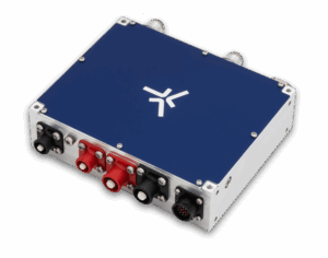
Figure 1: Brighloop DC-DC (Source: Brightloop)
GaN Devices Enable Higher Density and Faster Control
The collaboration with EPC played a central role in enabling BrightLoop’s switching strategy.
Rather than using silicon MOSFETs, BrightLoop selected EPC’s enhancement-mode GaN FETs to support operation at 600 kHz – substantially above the switching frequencies typically associated with comparable high-power silicon converters.
“Our initial selection for this design was the EPC2302,” said BrightLoop. “We chose it for its exceptionally low RDS(on), which is critical for reducing conduction losses at high currents.”
According to BrightLoop, thermal performance was equally important. The thermally enhanced package helped improve heat extraction while the higher breakdown voltage expanded the converter’s safe low-voltage operating range.
The company is now validating EPC2361 devices to further improve power density and reduce conduction losses.
“We are currently validating the EPC2361, which offers an even lower RDS(on), enabling us to achieve higher power density with further reduced losses,” BrightLoop added.
The move to GaN introduced benefits extending far beyond efficiency gains.
“The significant reduction in parasitic capacitances offered by GaN technology compared to traditional Silicon MOSFETs has been a major system-level differentiator,” said BrightLoop. “It enables us to increase the switching frequency from the typical 100–300 kHz range up to 600 kHz and beyond.”
Higher switching frequencies reduce passive component volume, enabling more compact magnetics and higher overall power density. Equally important, faster switching enables tighter digital control loops and significantly improved transient response.
“From a control standpoint, the higher switching frequency provides a much faster dynamic response, allowing the converter to handle transient events with superior bandwidth and agility,” BrightLoop said.
A switching frequency of 600 kHz in conjunction with high-bandwidth real-time digital control ensures stability over extreme conversion ratios. The ultra-fast switching speed enables us to reach a high control loop bandwidth. This enables our digital controller to react dynamically to high dv/dt and di/dt events. This ensures accurate regulation, high transient response and smooth bidirectional transitions with no danger of instability or control saturation.
Co-Engineering Reliability at High dv/dt
Wide-bandgap adoption introduces new challenges alongside its advantages. Faster switching transitions increase dv/dt and di/dt stress, making reliability increasingly dependent on layout parasitics, thermal design, and gate-drive optimization rather than nominal semiconductor ratings alone.
To address this, EPC and BrightLoop collaborated during the design phase rather than after hardware completion.
“Prior to final PCB layout and schematic validation, Brightloop engaged in a collaborative design review with EPC’s engineering team,” BrightLoop explained. “This joint effort focused on optimizing the gate driver circuitry, selecting appropriate magnetic components for high frequency operation, and defining the optimal switching speeds.”
This co-engineering process proved particularly valuable for ensuring robustness under worst-case operating conditions.
“Because device reliability in extreme operating environments is heavily influenced by layout parasitics and thermal dissipation, EPC’s feedback was invaluable in fine-tuning our thermal and electrical margins,” said BrightLoop.
The collaboration also extended into electromagnetic compatibility (EMC) optimization—often one of the most difficult aspects of high-frequency GaN power conversion.
“To manage the high dv/dt and di/dt transitions inherent to fast GaN switching, extensive PCB layout optimization was conducted to minimize parasitic power loop inductance,” BrightLoop explained. “Lowering this loop inductance significantly curtails voltage ringing and electromagnetic radiation.”
BrightLoop employed advanced PCB technologies, including micro-vias and blind vias, to physically isolate high-power switching loops from gate-driver circuitry, minimizing electromagnetic coupling and preserving gate-drive integrity.
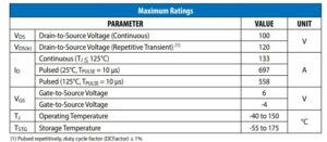
Figure 2: EPC2361 – Enhancement Mode Power Transistor features (Source: EPC)
Stability in Real Machines, Not Ideal Benches
Laboratory conditions rarely reflect real deployment environments. In electrified vehicles and industrial systems, converters must interact with batteries, long cable harnesses, and dynamic loads capable of introducing instability.
According to BrightLoop, cable parasitics emerged as one of the most important external variables affecting converter behavior.
“The most critical external parameter affecting system stability is the length of the external cables, which introduces significant parasitic line inductance,” the company said. “This inductance, excited by fast current transients, interacts with the system to create LC resonant circuits that generate severe voltage oscillations and ringing.”
To suppress these effects, additional bulk decoupling capacitance becomes essential for damping resonances and stabilizing input and output rails during transient events.
Fault handling also reflects the system-level focus of BrightLoop’s architecture. Rather than entering shutdown during overload or short-circuit events, the converter actively regulates current through an ultra-fast inner control loop.
“The BrightLoop converter does not trigger a shutdown or enter a fault state when a short-circuit or overload occurs,” said BrightLoop. “Instead, it utilizes an ultra-fast inner current limiting loop that actively regulates the current at its maximum allowable limit.”
From the point of view of the control theory, this loop is equivalent to an actuator saturation that limits the output to a safe maximum operating current value, without stopping the conversion process. This prevents the converter from tripping and ensures continuous operation while allowing the system to recover seamlessly as soon as the external fault or overload condition is cleared.
Centralized or Distributed Power?
In the transition to zonal vehicle electrical architectures and higher battery voltages, the role and location of DC-DC conversion is changing too. The system level requirements are expected to have both centralized and distributed high voltage to low voltage conversion strategies co-existing in the system.
In high constrained space and weight applications (e.g. high performance vehicles) centralized power conversion architectures are often preferred to ease packaging and improve power density. For applications such as aerospace, maritime, and heavy-duty transportation, distributed DC-DC converter architectures may be preferred to increase redundancy, improve fault isolation, and support safety-critical low-voltage networks.
The choice of wide-bandgap technologies in DC-DC power conversion is part of a larger engineering trend: optimizing the performance of a system is not just about swapping out silicon devices. The efficient implementation becomes more and more dependent on the co-optimization of semiconductor devices and switching behavior, thermal management, PCB layout, electromagnetic compatibility and control strategies.
With the evolution of electrified systems to higher operating voltages and more dynamic load profiles, DC-DC converters are playing an increasingly important role in overall power architecture, enabling energy distribution, subsystem isolation and power management across the platform.
Huawei Technologies has outlined a new semiconductor design and manufacturing approach that the company claims could reduce its dependence on advanced lithography equipment subject to US export controls. The announcement was made during the International Symposium on Circuits and Systems (ISCAS) in Shanghai by He Tingbo, head of Huawei’s semiconductor division.
Since 2019, Huawei has faced a series of US-led sanctions that have limited the company’s access to advanced semiconductor technologies, including extreme ultraviolet (EUV) lithography systems used for manufacturing leading-edge chips below the 5 nm process node. These restrictions have significantly affected China’s ability to produce the most advanced AI and high-performance computing processors domestically.
During the presentation, Huawei stated that it expects to produce next-generation 1.4 nm chips by 2031, positioning its roadmap close to that of leading foundries such as TSMC, which has projected similar capabilities by 2028.
Huawei’s proposed approach departs from traditional semiconductor scaling models based on Moore’s Law, the long-established principle stating that transistor density on integrated circuits doubles approximately every two years. Instead of focusing primarily on reducing transistor dimensions, Huawei introduced what it calls the “Tau Scaling Law,” also referred to as “Her’s Law.” The concept shifts optimization priorities toward reducing communication latency between functional blocks inside a processor rather than exclusively maximizing transistor density.
According to the company, this architectural approach addresses some of the physical limitations associated with continued transistor miniaturization, including power density, signal integrity and manufacturing complexity. Huawei stated that the new methodology enables competitive performance while potentially reducing reliance on EUV-based process scaling.
The company also revealed that the next generation of its Kirin processors, expected to launch later this year, will be the first products to adopt a new “LogicFolding” architecture based on the Tau Scaling concept. Huawei claims the design improves internal data communication efficiency and supports future AI-oriented workloads.
Industry analysts view the announcement as a signal that Huawei is pursuing alternative semiconductor development paths to mitigate the impact of export restrictions and strengthen China’s domestic semiconductor ecosystem. The company’s long-term roadmap is also expected to intensify competition and geopolitical tensions surrounding advanced AI and semiconductor technologies.
indie Semiconductor has signed a definitive agreement to acquire the fabless CMOS image sensor product line of ams OSRAM for a total consideration of €40 million. The acquisition expands indie’s sensing portfolio for automotive ADAS and supports the company’s growth strategy in physical AI and industrial vision applications.
The acquired business, with operations primarily located in Belgium and Portugal, develops high-performance CMOS image sensors for industrial automation, robotics, and AI-enabled vision systems. The portfolio includes products, intellectual property and design assets that complement indie’s existing sensing technologies across radar, LiDAR, ultrasonic and camera-based systems.
CMOS image sensors are increasingly important in sensor-intensive platforms such as humanoid robots, collaborative robots, and industrial automation equipment, where low latency, high resolution, and multimodal sensing are critical requirements. Market growth is also being driven by the expansion of AI-based vision systems and advanced driver assistance systems (ADAS), alongside rising automation and safety requirements across industrial and automotive markets.
Under the terms of the agreement, indie Semiconductor will pay €35 million in cash at closing, while ams OSRAM will provide a €5 million vendor debt note. The transaction remains subject to customary regulatory approvals and closing conditions and is expected to close during the third quarter of 2026.
According to the companies, the acquisition is expected to be immediately accretive and further strengthen indie’s position in high-performance sensing solutions for automotive and industrial applications.
Asahi Kasei has developed a new photosensitive polyimide (PSPI) film designed to support advanced panel-level semiconductor packaging, addressing the growing demand for higher manufacturing efficiency and improved production yields in next-generation semiconductor applications.
As semiconductor packaging technologies continue to evolve toward larger panel formats and increasingly complex multilayer structures, panel-level packaging has emerged as a key approach for improving scalability and cost efficiency. To respond to these industry trends, Asahi Kasei combined the characteristics of its existing PSPI materials and dry film photoresist (DFR) technologies into a newly engineered photosensitive film solution. The company confirmed that the material is currently undergoing customer evaluations and that commercial availability is expected in the near future.
The new PSPI film leverages Asahi Kasei’s expertise in PIMEL™ liquid PSPI materials, widely used for semiconductor buffer coatings and passivation layers, as well as its SUNFORT™ dry-film photoresist technology, commonly used for temporary lithographic circuit patterning on substrates and wafers.
According to the company, the newly developed film is intended to improve semiconductor packaging productivity by enabling more uniform and efficient lamination across large square panels. The material is also designed to support more insulating layers, helping manufacturers meet the increasing complexity of advanced packaging architectures. Potential applications include redistribution layers in semiconductor packages and insulating layers in package substrates.
Asahi Kasei stated that combining the PSPI film with the SUNFORT™ TA series, which supports circuit formation down to 1.0 μm line widths, allows both fine wiring patterns and insulating resin layers to be formed through film lamination processes. The company is also developing additional solutions integrating the PSPI film with the SUNFORT™ CX series to enable the formation of high-aspect-ratio copper pillars required for advanced three-dimensional semiconductor packaging technologies.
The development aligns with Asahi Kasei’s broader strategy to expand its electronics business, identified as a key growth area in the company’s medium-term management plan, Trailblaze Together. Materials such as PIMEL™ PSPI and SUNFORT™ dry film photoresist already play important roles in advanced semiconductor packaging processes.
Demand for high-performance packaging materials continues to increase as AI data centers drive the need for denser chip integration, larger interposers, and more sophisticated packaging structures. The industry transition from wafer-level packaging to panel-level and increasingly three-dimensional packaging architectures is also accelerating the need for finer wiring patterns, additional layers, and higher-performance insulating materials.
Imec has demonstrated the world’s first quantum dot qubit device fabricated using High NA EUV lithography. This marks a milestone toward industrial-scale production of reliable qubits for quantum computers.
Quantum computers offer exponential performance advantages over classical systems for specific tasks such as drug discovery and physical process simulation. Practical quantum computing, however, requires scaling to millions of interconnected qubits with high reliability and precise control.
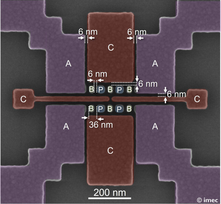
Among existing quantum platforms, silicon quantum dot spin qubits are considered promising for industrial scaling due to their compatibility with standard CMOS manufacturing processes. These “industry qubits” confine an electron within a silicon nanostructure; the electron’s spin state stores quantum information. Minimizing gaps between control gates is essential to reducing environmental noise.
Imec has fabricated a functional qubit network with gate gaps of just 6 nm using High NA EUV lithography. At this nanoscale, millions of qubits could theoretically be integrated onto a single chip.
This achievement builds on imec’s prior work with silicon quantum dot spin qubits, which already demonstrated low charge noise and stable operation using CMOS-compatible processes. By integrating High NA EUV lithography, the focus shifts from lab-scale individual devices to reproducible, 300 mm fab-compatible qubits.
While High NA EUV lithography is already recognized as essential for sub-2 nm logic and high-density memory that support advanced AI and high-performance computing, this result also confirms its critical role in future quantum computing hardware.