
IBM Advances U.S. Quantum Chip Manufacturing

0

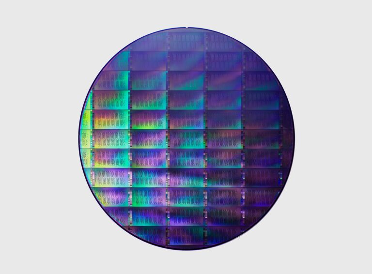
IBM and the U.S. Department of Commerce have announced a Letter of Intent (LOI) to establish the first purpose-built quantum chip foundry in the United States, marking a major step toward strengthening the country’s leadership in quantum technology and semiconductor manufacturing. The initiative, backed by a proposed $1 billion award under the CHIPS Act, is intended to accelerate domestic quantum research, development, and wafer production for a broad ecosystem of quantum hardware companies.

The CHIPS funding would support the creation of Anderon, a new standalone company formed by IBM to operate as a dedicated quantum wafer foundry. Alongside the proposed federal support, IBM plans to invest an additional $1 billion in cash and contribute intellectual property, manufacturing assets, and experienced personnel. Additional investors are expected to participate as the company expands.

Headquartered in Albany, New York, Anderon is expected to become America’s first pure-play quantum foundry, operating advanced 300-millimeter wafer manufacturing lines tailored specifically for quantum technologies. The project represents one of the largest U.S. government-backed quantum R&D efforts to date and is designed to help position the United States as a global leader in scalable quantum wafer manufacturing.

IBM emphasized that its broader quantum computing roadmap remains unchanged. The company stated that the new foundry initiative builds upon decades of expertise in both quantum computing and semiconductor fabrication. IBM has already demonstrated scalable quantum wafer technologies internally, creating a foundation for future commercialization and high-volume production.

As a dedicated foundry provider, Anderon plans to manufacture wafers for a variety of quantum technology developers worldwide. Initially, the company will focus on superconducting qubit wafers and associated supporting electronics, while future expansion plans include support for additional quantum computing modalities.

The foundry is also intended to strengthen the domestic supply chain for quantum hardware by providing a secure U.S.-based source for advanced quantum wafers. IBM aims to leverage its process expertise, manufacturing infrastructure, and specialized workforce to help establish reliable quantum production capabilities within the country.

According to the announcement, Anderon’s future manufacturing platform will support advanced 300mm quantum wafer technologies, including superconducting interconnects, through-silicon vias, and bump technologies. The facility is also expected to include sophisticated process design kits, inline testing and characterization capabilities, and baseline manufacturing flows that support rapid development cycles and scalable production.

Quantum computing is widely viewed as a transformative paradigm capable of solving highly complex scientific and industrial problems that classical supercomputers cannot solve. Potential applications span materials discovery, chemistry, optimization, cybersecurity, and advanced simulations.

IBM highlighted its longstanding leadership in the quantum sector, noting that it has deployed more than 90 quantum systems globally and maintains a network of over 325 Fortune 500 companies, research institutions, startups, and government agencies using its quantum computing infrastructure. The company has also collaborated extensively with organizations such as the National Institute of Standards and Technology, the Defense Advanced Research Projects Agency, and the United States Department of Energy to advance secure quantum manufacturing and large-scale fault-tolerant quantum computing.

IBM reiterated its goal of delivering the world’s first commercially useful large-scale fault-tolerant quantum computer by 2029. The launch of Anderon remains subject to final agreements and regulatory processes between IBM and the Department of Commerce following the newly announced Letter of Intent.

Why Bosch Needs Two SiC Module Lines to Solve One Inverter Problem

Every EV platform team faces a version of the same spreadsheet problem: cover compact cars at ~80 kW and performance vehicles above 400 kW, across 400 V and 800 V architectures, with as few hardware variants as possible. The traction inverter sits at the center of that spreadsheet. And the power module inside the inverter is the component that determines how many rows it actually has.

Bosch just made that calculation more explicit. The company published detailed technical positioning for two distinct SiC power module families — PM6 and DSL — designed for the same traction inverter market but optimized for fundamentally different scaling strategies.

PM6 packs up to twelve SiC chips into a single half-bridge package; DSL keeps just two chips per module and lets the system integrator decide how many to parallel. The fact that Bosch ships both tells you something about where the inverter design conversation has moved.

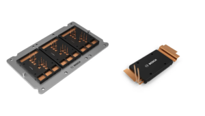
Figure 1: Bosch SiC power module portfolio for traction inverters. Source: Bosch Semiconductors.


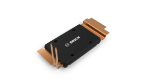
Figure 2: PM6 power module. Source: Bosch Semiconductors.

PM6 is Bosch’s answer for the mainstream high-voltage traction inverter. Each module forms a half bridge with two topological switch positions. Three PM6 modules make a complete three-phase B6 bridge, covering roughly 80 kW to over 400 kW.

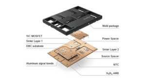
The scaling happens inside the package. Depending on the power target, a PM6 module can integrate four, eight, or twelve SiC MOSFET chips, with die sizes up to 40 mm² each. Per topological switch, that means two, four, or six chips in parallel. An OEM designing a compact EV and a performance SUV on the same inverter platform can use the same module footprint with different chip populations.

This matters because Bosch positions PM6 scaling inside the module rather than through multiple external modules in parallel, reducing the number of platform variants and the related development burden. For platform teams managing several vehicle variants, that points to fewer hardware variants, reduced development effort, and easier production scaling.

The thermal and electrical design reinforces the platform logic. Silicon nitride (Si₃N₄) ceramic substrates handle both heat extraction and thermal cycling stress. A symmetrical internal layout suppresses stray inductance and voltage overshoot — the two parameters that most directly limit how fast you can switch SiC MOSFETs in practice. Bosch’s PM6 materials also state that the platform supports both open pin-fin and closed strip-fin coolers, in aluminum or copper, depending on the required performance. The module accommodates the cooling architecture rather than dictating it.

DSL: more modules, more topological freedom


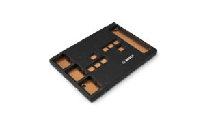
Figure 3: DSL power module. Source: Bosch Semiconductors.


DSL takes the opposite approach. Each module contains just two parallel SiC MOSFETs — a single switch element. A basic B6 bridge needs six DSL modules. Higher power? Parallel two per position (twelve total), three (eighteen), or four (twenty-four).

The design point is flexibility. DSL modules can populate conventional B6 topologies, but they also fit multilevel circuits and other architectures where the switching building block needs to be smaller than a half bridge. For OEMs exploring topologies beyond standard three-phase bridges — and several are, especially for 800 V and future 1200 V systems — DSL provides a way to prototype and validate without committing to a custom module.

There is a practical consideration as well. Smaller or more space-constrained applications — including two-wheelers and other individually designed high-voltage functions — may only need the power of a single DSL per switch position. The module’s compact form factor accommodates constrained installation spaces that a PM6 physically cannot fit into.

Two customer camps split on inverter architecture — Bosch ships a product for each

Bosch could have designed one module family with a wider scaling range. The decision to maintain two lines reflects a structural reality in the inverter market: OEMs do not agree on how to build traction inverters.

Some vehicle manufacturers are committed to conventional B6 architectures and want the fewest possible part numbers across their entire EV lineup — exactly the consolidation logic PM6 was designed around. Others are investing in advanced topologies — multilevel, modular, or application-specific — where the power module needs to be a building block rather than a pre-integrated subsystem, and DSL gives them that granularity.

Trying to force both use cases into a single module family would mean compromising either power density or topological flexibility. Bosch’s two-line approach accepts that the traction inverter market is diverging, and positions a product for each branch.

Gen 3 SiC chips and the Fuji Electric dual-source deal

The module portfolio connects to two other layers of Bosch’s SiC strategy that are easy to overlook.

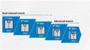
First, the chip roadmap. Bosch recently introduced its third-generation SiC trench MOSFETs, with samples already shipping to global automakers. Each chip generation feeds directly into the module platform: better specific on-resistance means fewer chips per switch position for the same current rating, which means either smaller modules or higher power in the same footprint.

Second, the Fuji Electric collaboration. Announced in late 2025, the partnership targets mechanical package compatibility — matching outer dimensions and terminal positions between Bosch and Fuji Electric SiC modules. For OEMs, that creates a dual-source option at the module level with significantly reduced mechanical adaptation effort — a meaningful risk-reduction path once both options pass the required automotive qualification work.

Bosch’s global production network — spanning Europe, Asia, and the Americas — supports a local-for-local supply model. For automotive programs, that geographic diversification strengthens the supply-chain argument around the module portfolio.

Three open variables for next-generation platform decisions

Three questions will determine whether PM6 and DSL actually change how a traction inverter program runs.

Chip generation cadence. Bosch’s Gen 3 SiC MOSFETs are sampling now. How quickly those devices move into PM6 and DSL production modules — and what that does to the power-per-footprint curve — directly affects platform planning for 2028–2030 vehicle programs.

Figure 4: Bosch Gen 3 SiC chip update. Source: Bosch.


Fuji Electric interchangeability timeline. The collaboration is announced but the timeline for qualified, interchangeable modules has not been disclosed. Until dual-source modules pass automotive qualification in parallel, the supply chain benefit remains a design intent.

Figure 5: Bosch and Fuji Electric power module exchangeability. Source: Bosch Semiconductors.


Topology adoption rate. DSL’s value proposition scales with how many OEMs actually move beyond B6. Should the industry stay on standard three-phase bridges for the next decade, DSL remains a specialist option. The calculus reverses once multilevel or modular topologies gain real traction at 800 V and above — at that point, DSL’s per-switch granularity could make it the more strategically important line.

The power module used to be the part of the inverter you specified last. Bosch is betting it becomes the part you specify first.


Sources:

Thales Demonstrates Quantum Link in Canary Islands

0

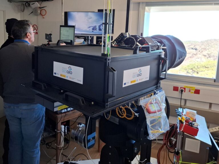
Thales Alenia Space and its project partners have successfully completed a high-precision quantum communication transmission between the Canary Islands of La Palma and Tenerife as part of the Spanish GEO QKD initiative. The achievement represents a major milestone in the development of Europe’s future space-based quantum key distribution (QKD) infrastructure.

The GEO QKD project aims to develop the first quantum key distribution system operating from geostationary orbit. The recent field tests were designed to validate the technology in a real-world environment before deployment aboard a satellite.

The demonstration used an engineering model replicating both the satellite payload and the associated ground segment. The QKD payload was installed at the Roque de los Muchachos Observatory, while the terrestrial optical receiver was located at the Teide Observatory.

During the tests, the teams successfully transmitted quantum key distribution signals consisting of individual photons through free space over a distance of approximately 140 km under atmospheric turbulence. The transmitted signal was then injected into a single-mode optical fiber measuring only 10 microns in diameter. According to the project participants, this level of precision in free-space quantum transmission had not been demonstrated before.

The project team reported successful completion of all major operational phases, including calibration, synchronization, and photon transmission protocols. The results demonstrated the system’s stability and robustness and confirmed the practical feasibility of long-distance quantum communication technologies for future satellite deployment.

Over the coming months, the consortium plans to continue testing and refining the system in the Canary Islands to further validate performance and prepare for future space-based implementation. The project is intended to contribute to Europe’s digital sovereignty by enabling a highly secure quantum-encrypted communications infrastructure.

The GEO QKD initiative is supported by the Spanish State Secretariat for Telecommunications and Digital Infrastructure, managed by the Center for Technological Development and Innovation (CDTI), and funded through European Union recovery programs under the PERTE Aeroespacial initiative.

Toshiba Samples SmartMCD™ IC Integrating MCU & MOSFET for BLDC Motors

0

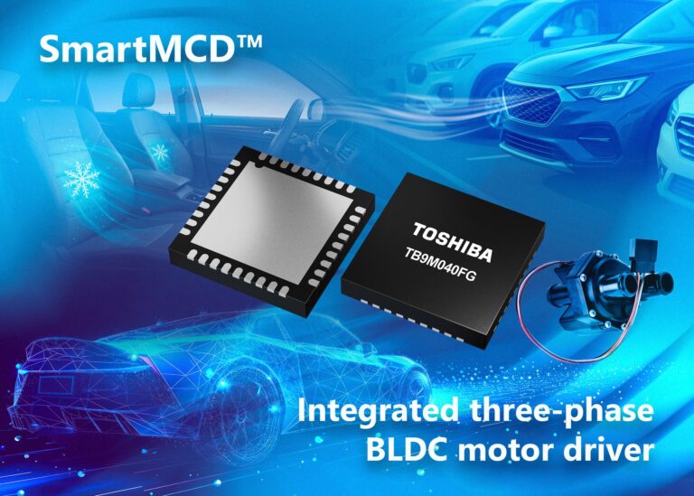
Toshiba Electronics Europe GmbH has initiated shipments of engineering samples of the TB9M040FTG SmartMCD™ device. This product integrates a microcontroller (MCU) and power MOSFETs to directly drive three-phase brushless DC (BLDC) motors in compact automotive systems up to 40W.

Rising vehicle electrification increases demand for small BLDC motors in electric valves, HVAC dampers, pumps, fans, and grille shutters. These applications require high integration to reduce component count and minimize ECU size.

The TB9M040FTG incorporates a 32-bit Arm® Cortex®-M23 core, flash memory, a three-phase BLDC driver with integrated MOSFETs, a 5V supply for external sensors, and a LIN transceiver—all within a 6mm × 6mm VQFN36 package.

A dedicated Vector Engine (VE) coprocessor accelerates field-oriented control (FOC), shortens FOC cycle times, reduces CPU load, and minimizes software footprint. Back electromotive force (BEMF) detection enables sensorless square-wave control.

The device meets AEC-Q100 Grade 0 and supports ASIL-B, targeting automotive applications with medium functional safety requirements. Integrated protection includes undervoltage, overvoltage, overcurrent, thermal shutdown, charge pump monitoring, and drain-source voltage (Vds) detection for high- and low-side MOSFETs.

Toshiba will extend the SmartMCD™ series to enable compact, efficient automotive motor control systems.

Further information is available on the product webpage.

NoMIS Joins ARPA-E Project with 3.3 kV SiC MOSFETs

0

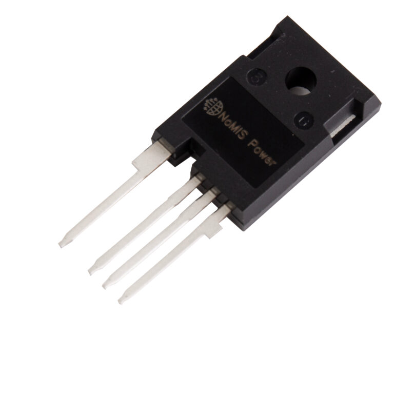
NoMIS Power Corporation has joined a U.S. Department of Energy-backed consortium developing next-generation high-voltage DC transmission technologies under the Advanced Research Projects Agency–Energy (ARPA-E) DC-GRIDS program. The three-year, $2.5 million project is led by Michigan State University and focuses on developing silicon carbide-based Neutral Point Clamped Power Electronics Building Blocks (NPC-PEBBs) for modular high-voltage direct current (HVDC) converters.

The project will leverage NoMIS Power’s portfolio of 3.3 kV silicon carbide (SiC) MOSFETs, including the company’s upcoming 25 mΩ device, to support the development of 6.6 kV / 2.5 kA NPC-PEBB submodules for multiport multiterminal HVDC (MT-HVDC) systems. According to the consortium, the technology is intended to improve efficiency, power density, reliability, and fault protection in future HVDC infrastructure.

The ARPA-E DC-GRIDS initiative focuses on accelerating the development of advanced DC power conversion technologies that expand transmission capacity for applications such as electrification, offshore wind integration, interregional grid connections, and rapidly growing data center power demand.

The consortium includes several industry and research organizations, such as the Electric Power Research Institute (EPRI), OPAL-RT Technologies, GE Grid Solutions, the National Renewable Energy Laboratory (NREL), Salt River Project, and Minnesota Power.

The NPC-PEBB architecture is designed as a vendor-agnostic, plug-and-play submodule for modular HVDC converters. Compared with conventional silicon IGBT-based half-bridge submodules, the SiC-based design offers a three-level 6.6 kV output, full DC fault current blocking capability, and a 60% reduction in capacitor size through advanced multilevel modulation techniques.

NoMIS stated that its upcoming 25 mΩ 3.3 kV SiC MOSFET is particularly well-suited for HVDC submodule applications because its low on-resistance can significantly reduce conduction losses, while improving converter efficiency and thermal performance at high operating currents.

As part of the project, NoMIS Power will lead SiC device-level packaging activities, electrical testing, screening, and performance characterization for the power devices and modules integrated into the NPC-PEBB assemblies. The work will be carried out at the company’s facility within the Albany Nanotech Complex.

Beyond the consortium, NoMIS confirmed that its 3.3 kV SiC MOSFETs and power modules will also be available to other DC-GRIDS participants and external medium- and high-voltage power electronics developers seeking to transition from legacy IGBT-based systems to silicon carbide technologies.

Cyient Semiconductors Launches India’s First GaN Power IC Family

0

Cyient Semiconductors Private Limited has launched seven gallium nitride (GaN) power devices for the Indian market. The devices are developed using licensed technology from Navitas Semiconductor. This release represents Cyient Semiconductors’ first commercial GaN product family.

The portfolio targets Edge AI computing, e-mobility, AI data centers, telecommunications, consumer fast charging, industrial power systems, and e-mobility platforms.

A strategic collaboration announced in December 2025 enables Cyient to license Navitas’s proven GaN technology for use in India. Under the agreement, Cyient will also serve as a second source for select Navitas GaN devices already in mass production, strengthening supply chain resilience.

Compared to silicon-based power semiconductors, GaN devices offer higher switching speeds, lower conduction losses, improved thermal efficiency, reduced power losses, smaller solution size, simplified thermal management, and increased overall system performance.

The initial GaN portfolio operates at voltages up to 650 V. Target applications include consumer USB-PD chargers, laptop and mobile adapters, AC-DC power supplies, AI data center and telecom power systems, and e-mobility charging platforms.

The first wave includes seven highly integrated GaN power devices in DPAK packages. These combine drive, control, protection, integrated EMI management, and current sensing. This integration simplifies system design and reduces time-to-market.

Cyient Semiconductors plans to expand its GaN portfolio through partnerships with local OSATs (outsourced semiconductor assembly and test providers). The licensing agreement with Navitas is intended to enable domestic manufacturing of GaN power devices in India over time. Sampling of the first GaN power products is expected to begin by June 2026.

Google Quantum AI Identifies Cause of Radiation-Induced Error Bursts in Superconducting Qubits

0

Researchers have identified the mechanism behind persistent error bursts in superconducting quantum computers, even when protected by gap engineering. The findings are published in “Physical Review X” by Vladislav Kurilovich and colleagues at Google Quantum AI.

Superconducting qubits are vulnerable to ionizing radiation from space or environmental sources. Radiation particles interact with the silicon substrate, generating quasiparticles that disrupt qubit operation. Gap engineering creates an energy barrier in the superconducting material to prevent quasiparticle tunneling.

Despite this defense, sudden widespread errors affecting multiple qubits simultaneously have been observed. The cause was previously unknown.

The team developed a rapid measurement protocol using a 72-qubit Willow processor. They performed repetitive qubit measurements every few microseconds to capture error bursts in real time.

Results showed that while quasiparticles do not tunnel through the energy barrier, they induce qubit frequency shifts of up to 3 MHz. This detuning causes qubits to lose synchronization with the microwave control pulses. The consequence is accumulated phase errors and incorrect shifts in the quantum state.

This mechanism explains a previous observation from Google experiments: a logical error rate (LER) floor, at which error correction no longer improves performance despite additional mitigation efforts.

As a countermeasure, the researchers implemented echo pulses, additional control operations that cancel unwanted phase shifts. This approach reduces system sensitivity to radiation-induced frequency fluctuations.

Firgun Ventures Joins $160M Series C in Quantum Motion for Silicon-Based Quantum Computing

0

Firgun Ventures, a $250 million quantum technology fund, has made its first European investment. The firm is participating in a $160 million Series C funding round for Quantum Motion, a London-based quantum computing company. Co-leads include DCVC and Kembara. Other participants are the British Business Bank, Oxford Science Enterprises, Inkef, Bosch Ventures, Porsche Automobil Holding SE, and Parkwalk Advisors.

Quantum Motion develops full-stack quantum computers using standard 300 mm silicon CMOS fabrication processes—the same technology used in conventional semiconductors. The architecture is designed to scale to millions of qubits, enabling fault-tolerant and commercially viable quantum computing.

The investment marks Firgun’s entry into the European market. Previous Firgun investments include Photonic Inc. (distributed quantum computing and communications) and Quantum Elements (an AI platform for quantum applications).

Quantum Motion was founded in 2017 by Professor John Morton (UCL) and Professor Simon Benjamin (University of Oxford). The company employs more than 100 people across the UK, the US, Australia, and Spain. In September 2025, Quantum Motion demonstrated the world’s first full-stack quantum computer built on standard silicon chips. That system is now deployed at the UK National Quantum Computing Center (NQCC) for research applications, including drug discovery.

Additionally, Quantum Motion was selected to advance to Stage B of the US Defense Advanced Research Projects Agency (DARPA) Quantum Benchmarking Initiative (QBI) in late 2025.

Prior to this Series C, the company raised over £62 million in equity and grant funding. That included an oversubscribed £42 million Series B led by Bosch Ventures and Porsche SE, which supported the expansion and development of silicon quantum processors.

Uviquity Introduces Chip-Scale 229 nm Deep-UV Laser

0

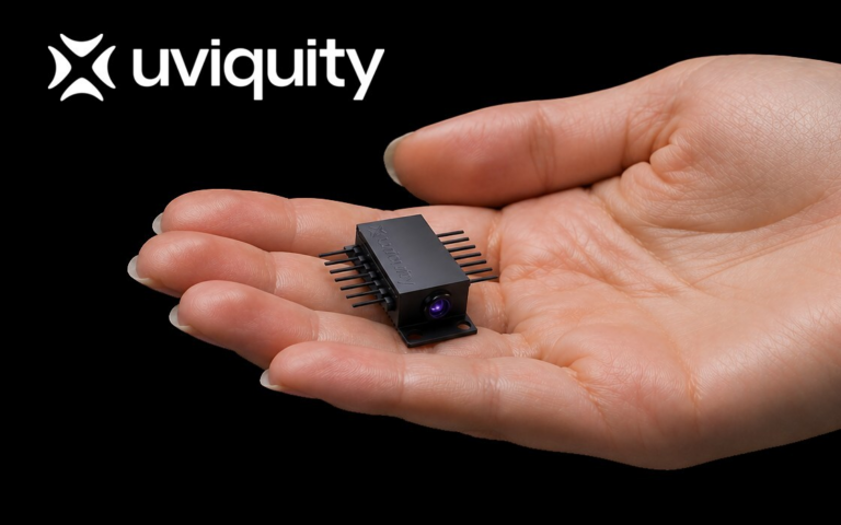
Uviquity has released its first product: a chip-scale laser operating at 229 nm. This device is the first single-semiconductor-chip laser at this wavelength, providing collimated, narrow-linewidth, spectrally pure output. Sampling to OEM partners begins in Q4 2026. Target applications include semiconductor manufacturing, pharmaceutical and biopharmaceutical production, petrochemical processing, environmental monitoring, and defense.

The laser is built on an aluminum nitride (AlN) photonic integrated circuit (PIC) platform. It generates deep-UV output via second harmonic generation (SHG) in proprietary AlN waveguides. The technology is protected by over 20 pending patents and was first presented at SPIE Photonics West in January 2026. Uviquity currently holds the shortest-wavelength SHG record in AlN. The same platform supports far-UVC disinfection products for air, food, water, and medical applications, enabling both deep-UV sensing and disinfection markets with a single semiconductor architecture.

At 229 nm, the laser enables resonance-enhanced detection of biological and chemical signatures with minimal background fluorescence in most organic samples. It supports Raman, fluorescence, photoluminescence, and absorption spectroscopy.

Current deep-UV sources for instruments include lasers, lamps, and LEDs, each with trade-offs in spectral purity, brightness, lifetime, form factor, and cost. Many demanding applications require large, expensive benchtop systems. Uviquity’s laser delivers deep-UV performance from a chip in a compact, rugged, field‑deployable optoelectronic package that runs on low‑voltage power. It is suitable for handheld, in‑line, and embedded designs.

Application areas include semiconductor inspection and metrology, real‑time industrial process analytics, continuous gas analysis, reagent‑free water quality monitoring, and trace‑level defense sensing. Early‑access OEM sampling allocations for Q4 2026 are open.

STMicroelectronics Introduces VIPerGaN 100W GaN Converters

0

STMicroelectronics has released two new 100W VIPerGaN high-voltage converters, the VIPerGaN100W and VIPerGaN100WB. These monolithic gallium nitride (GaN) converters are designed for energy-efficient applications in domestic appliances, building automation, smart lighting, and consumer electronics such as televisions and device chargers.

The VIPerGaN100W features a 3.5A drain current limit, while the VIPerGaN100WB offers a 4.2A current limit, supporting peak power up to 125W. Both converters operate over a universal AC input voltage range (85V to 265V), delivering 100W at 185V. Each device integrates a 700V GaN power transistor with a low RDS(on) of 0.27mΩ to enhance thermal performance. The 5mm x 6mm QFN package includes the flyback converter and GaN gate driver, simplifying design.

The high switching-frequency capability of GaN transistors enables the use of smaller passive components, thereby optimizing energy efficiency and power density. ST has demonstrated this with the EVLVIPGAN100WP reference design for a 100W USB Type-C Power Delivery 3.0 adapter using the VIPERGAN100W. This reference design achieves over 92% peak efficiency and a power density of 24W/in³.

Both converters utilize a quasi-resonant flyback architecture with zero-voltage switching. Flexible power management techniques, including frequency foldback at light load and valley skipping at mid load, maintain efficiency across the load range. A proprietary valley lock feature in valley-skipping mode prevents variations in audio frequency. No-load power consumption is below 30mW due to burst-mode operation.

Integrated features include line-voltage feedforward for stable power delivery amid input-voltage fluctuations and dynamic blanking time to minimize switching losses. Protection mechanisms cover input and output overvoltage, overtemperature, brown-in, and brown-out.

The VIPerGaN100W and VIPerGaN100WB are available now.